Äîêóìåíòàöèÿ è îïèñàíèÿ www.docs.chipfind.ru
Preliminary Data Sheet
Vectron International, 267 Lowell Road, Hudson, NH 03051
Tel: 1-88-VECTRON-1
·
Web:
www.vectron.com
Page 1 of 8
Rev: 18Dec05
FX-424
Low Jitter Frequency Translator
Features
·
Quartz-based PLL for Ultra-Low Jitter
·
Frequency Translation up to 850 MHz
·
Accepts up to 4 ext.-muxed clock inputs
·
CMOS / LVDS / LVPECL Inputs compatible
·
Differential LVPECL or LVCMOS Output
·
Lock Detect / Loss of Signal Alarms
·
Output Disable
·
20.3 x 13.7 x 5.1 mm SMT package
·
RoHS/Lead Free Compliant
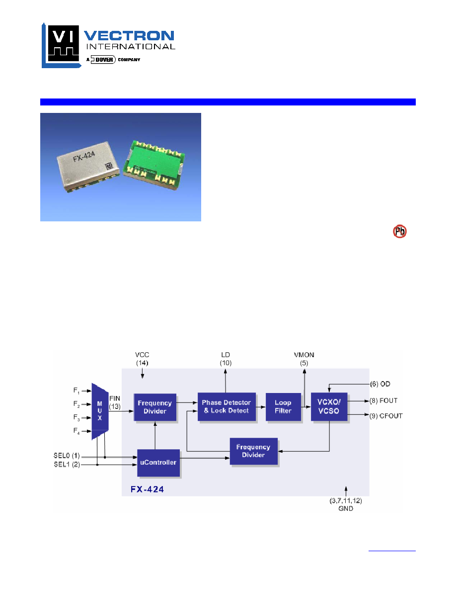
Description
The FX-424 is a precision quartz-based frequency
translator used to translate an input frequency such
as 8 kHz, 1.544 MHz, 2.048 MHz, 19.44 MHz etc.
to any specific frequency from 1.544 MHz to 850
MHz. The FX-424 can perform either up or down
frequency conversion. The FX-424's superior jitter
performance is achieved through the use of a
precision VCXO or VCSO. With the use of an
external multiplexer, up to 4 different input clocks
can be translated to a common output frequency.
Applications
·
Wireless Infrastructure
·
10 Gigabit FC
·
10GbE LAN / WAN
·
OADM and IP Routers
·
Test Equipment
·
Military Communcations
Figure 1. Functional Block Diagram
FX-424 Low Jitter Frequency Translator
Vectron International, 267 Lowell Road, Hudson, NH 03051
Tel: 1-88-VECTRON-1
·
Web:
www.vectron.com
Page 2 of 8
Rev: 18Dec05
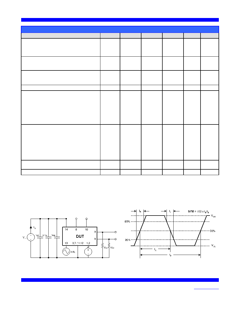
Table 1. Electrical Performance
Parameter
Symbol Minimum
Typical Maximum Units
Notes
Frequency
Input Frequency
Capture Range
Output Frequency
F
IN
APR
F
OUT
0.008
±
40
1.544
170
850
MHz
ppm
MHz
1,2,3
1,2,3
1,2,3
Supply
Voltage
Current (No Load)
V
CC
I
CC
3.13
3.3
45
3.46
60
V
mA
2,3
3
Input Signal
CMOS
LVPECL
F
IN
F
IN
CMOS
LVPECL
2,3
LVCMOS Output (Option
A
)
LVCMOS
2,3
Differential Output (Option
F
)
Common Mode Output Voltage
Output High Voltage
Output Low Voltage
Peak-to-Peak Output Voltage
Rise Time
Fall Time
Symmetry
V
OCM
V
OH
V
OL
V
P-P
t
R
t
F
SYM
V
CC
-1.5
V
CC
-1.025
V
CC
-1.810
45
V
CC
-1.3
V
CC
-0.950
V
CC
-1.700
700
0.5
0.5
50
V
CC
-1.1
V
CC
-0.880
V
CC
-1.620
55
V
V
V
mV-pp
ns
ns
%
2,3
2,3
2,3
2,3
4,5
4,5
2,3
SSB Phase Noise, F
OUT
= 155.52/622.08
@ 10 Hz Offset
@ 100 Hz Offset
@ 1 kHz Offset
@ 10 kHz Offset
@ 100 kHz Offset
@ 1 MHz Offset
@ 10 MHz Offset
n
n
n
n
n
n
n
-64/-27
-95/-55
-123/-85
-143/-110
-146/-130
-146/-146
-146/-146
dBc/Hz
dBc/Hz
dBc/Hz
dBc/Hz
dBc/Hz
dBc/Hz
dBc/Hz
5,6
Jitter Generation
J
50
ps RMS
5, 6
Operating Temperature
T
OP
-40 85
°C
1,3
1. See Standard Frequencies and Ordering Information.
2. Parameters are tested with production test circuit below (Fig 2).
3. Parameters are tested at ambient temperature with test limits guard-banded for specified operating temperature.
4. Measured from 20% to 80% of a full output swing (Fig 3).
5. Not tested in production, guaranteed by design, verified at qualification.
6. The FX-424 phase noise and jitter performance can be optimized for specific applications. Please consult with Vectron's Application
Engineers for more information.
Figure 2. Test Circuit
Figure 3. LVPECL Waveform
FX-424 Low Jitter Frequency Translator
Vectron International, 267 Lowell Road, Hudson, NH 03051
Tel: 1-88-VECTRON-1
·
Web:
www.vectron.com
Page 3 of 8
Rev: 12Dec05
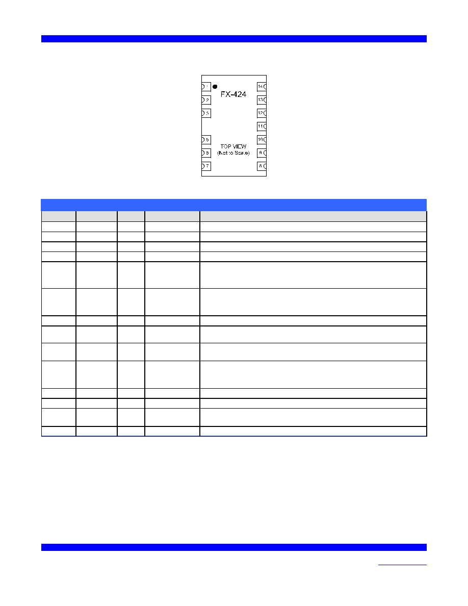
Figure 4. Pin Configuration
Table 2. Pin Out
Pin #
Symbol
I/O
Level
Function
1
SEL0 I LVTTL
Input Frequency Select*
2
SEL1 I LVTTL
Input Frequency Select*
3
GND GND Supply
Case and Electrical Ground
4
Not present
5
VMON O Analog
VCXO Control Voltage Monitor
Under locked conditions VMON should be > 0.3V and <3.0V. The input
frequency may be out of range if the voltage exceeds these levels.
6
OD I LVCMOS
Output Disable
Disabled = Logic "1"
Enabled = Logic "0" or no connect
7
GND GND Supply
Case and Electrical Ground
8
FOUT O
LVPECL or
LVCMOS
Frequency Output
9
CFOUT
O or
GND
LVPECL or
LVCMOS
Complementary Frequency Output Note for LVCMOS option this pad
will be tied to GND.
10
LD O LVCMOS
Lock Detect
Locked = Logic "1"
Loss of Signal = Logic "0"
11
GND GND Supply
Case and Electrical Ground
12
GND GND Supply
Case and Electrical Ground
13
FIN I
LVCMOS or
LVPECL
Input Frequency. The FX-424 series AC couples the input for handling of
either LVCMOS or LVPECL input signals.
14
VCC VCC Supply
Power Supply Voltage (3.3 V ±5%)
* For applications requiring two to four input frequencies, Vectron will assign a unique part number and the Input Frequency versus SEL[1:0]
settings will be provided in a Specification Control Drawing. For single input configurations it is recommended that SEL0 and SEL1 are tied
to ground.
FX-424 Low Jitter Frequency Translator
Vectron International, 267 Lowell Road, Hudson, NH 03051
Tel: 1-88-VECTRON-1
·
Web:
www.vectron.com
Page 4 of 8
Rev: 18Dec05
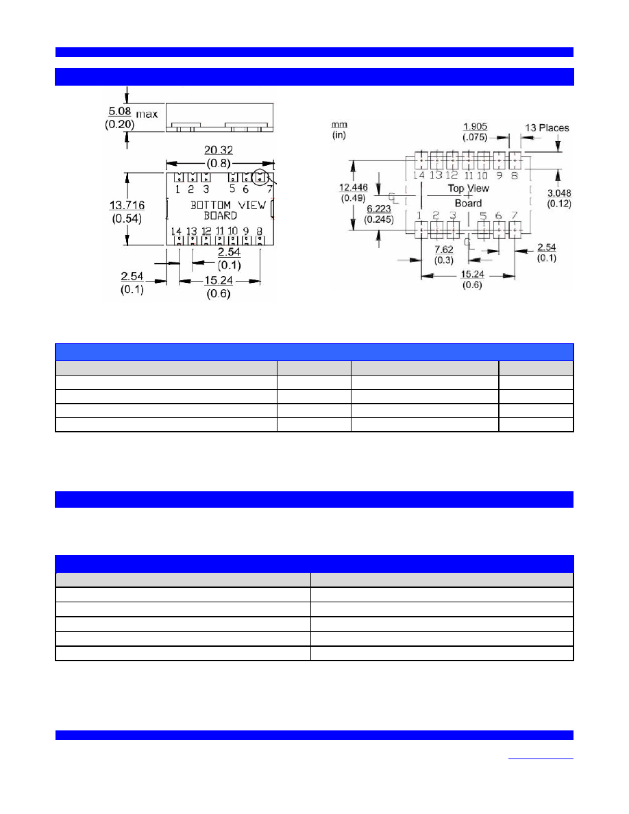
Outline Diagram
Suggested Pad Layout
Figure 5.
Figure 6.
Table 3. Absolute Maximum Ratings
Parameter
Symbol
Ratings
Unit
Power Supply
V
CC
0 to 6
V
Output Current
I
OUT
mA
Storage Temperature
TS
-55 to 125
°
C
Soldering Temp/Time
T
LS
260/40
°
C/sec
Stresses in excess of the absolute maximum ratings can permanently damage the device. Functional operation is
not implied at these or any other conditions in excess of conditions represented in the operational sections of this
data sheet. Exposure to absolute maximum ratings for extended periods may adversely affect device reliability.
Reliability
VI qualification includes aging at various extreme temperatures, shock and vibration, temperature cycling, and IR
reflow simulation. The FX-424 family is undergoing the following qualification tests:
Environmental Compliance
Parameter
Conditions
Mechanical Shock
MIL-STD-883, Method 2002
Mechanical Vibration
MIL-STD-883, Method 2007
Solderability
MIL-STD-883, Method 2003
Gross and Fine Leak
MIL-STD-883, Method 1014
Resistance to Solvents
MIL-STD-883, Method 2016
FX-424 Low Jitter Frequency Translator
Vectron International, 267 Lowell Road, Hudson, NH 03051
Tel: 1-88-VECTRON-1
·
Web:
www.vectron.com
Page 5 of 8
Rev: 12Dec05
The FX-424 is being qualified to meet the JEDEC
standard for Pb-Free assembly. The temperatures
and time intervals listed are based on the Pb-Free
small body requirements. The temperatures refer to
the topside of the package, measured on the package
body surface. The FX-424 should not be subjected to
a wash process that will immerse it in solvents. NO
CLEAN is the recommended procedure. The FX-424
has been designed for pick and place reflow
soldering. The FX-424 may be reflowed once and
should not be reflowed in the inverted position.
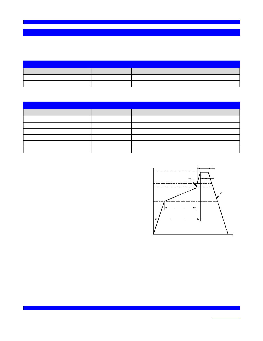
25
217
200
150
260
Te
mperat
ure (De
g
C)
Time (sec)
t
S
t
AMB-P
t
L
t
P
R
R
DN
eliability
Handling Precautions
Although ESD protection circuitry has been designed into the FX-424 proper precautions should be taken when
handling and mounting. VI employs a human body model (HBM) and a charged-device model (CDM) for ESD
susceptibility testing and design protection evaluation
ESD Ratings
Model
Minimum
Conditions
Human Body Model
500 V
MIL-STD 883, Method 3015
Charged Device Model
500 V
JEDEC, JESD22-C101
Reflow Profile (IPC/JEDEC J-STD-020C)
Parameter
Symbol
Value
PreHeat Time
t
S
60 sec Min, 180 sec Max
Ramp Up
R
UP
3
o
C/sec Max
Time Above 217
o
C t
L
60 sec Min, 150 sec Max
Time To Peak Temperature
t
AMB-P
480 sec Max
Time At 260
o
C
t
P
20 sec Min, 40 sec Max
Ramp Down
R
DN
6
o
C/sec Max
.