Äîêóìåíòàöèÿ è îïèñàíèÿ www.docs.chipfind.ru
Product Data Sheet
FX-500
Low Jitter Frequency Translator
Features
· Complete Frequency Translator to 77.760 MHz
· 3.3 Volt or 5.0 Volt Supply
· Capable of locking to an 8 kHz pulse/ BITS clock
· Tri-State Output allows board test
· Lock Detect
· J-Lead Ceramic Package
· Advanced Custom ASIC Technology
· Absolute Pull Range Performance to ±100 ppm
· CMOS Output
· Commercial or Industrial Temperature Range
· EIA Compatible Tape and Reel Packaging
Applications
· Frequency Translation, Clock Smoothing
· Telecom - SONET/SDH/ATM/DWDM
· Datacom - DSLAM, DSLAR, Access Nodes
· Cable Modem Head End
· Base Station - GSM, CDMA
Description
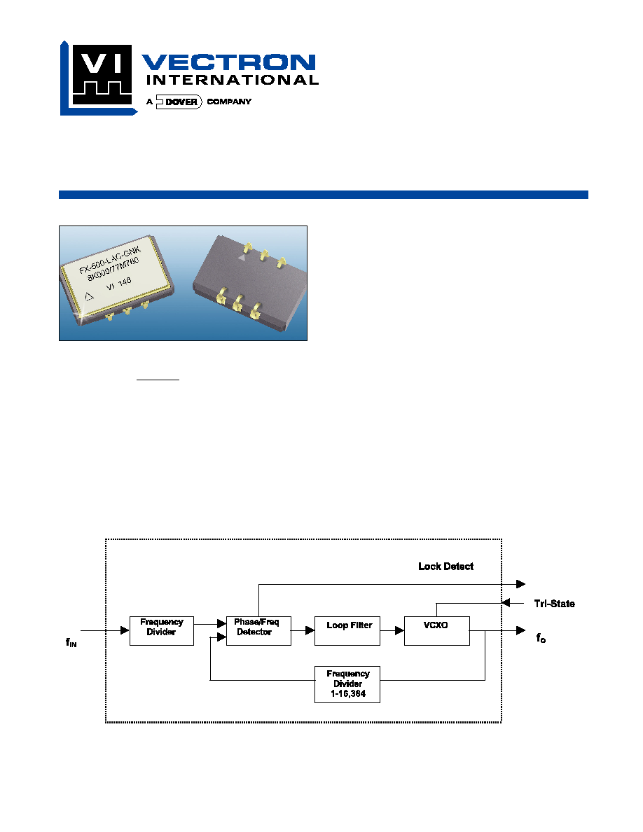
The FX-500 is a complete crystal-based frequency
translator used in communications applications
where low jitter is paramount.
Performance advantages include superior jitter per-
formance, high output frequencies and small pack-
age size. Advanced custom ASIC technology
results in a highly robust, reliable and predictable
device.
The device is packaged in a 6 pin J-Lead ceramic
package with a hermetic seam welded lid.
Figure 1. FX-500 Block Diagram
FX-500 Low Jitter Frequency Translator
Performance Characteristics
Electrical Performance
Vectron International ·
267 Lowell Road, Hudson, NH 03051 · Tel: 1-88-VECTRON-1 · Web: www.vectron.com
2
.
.
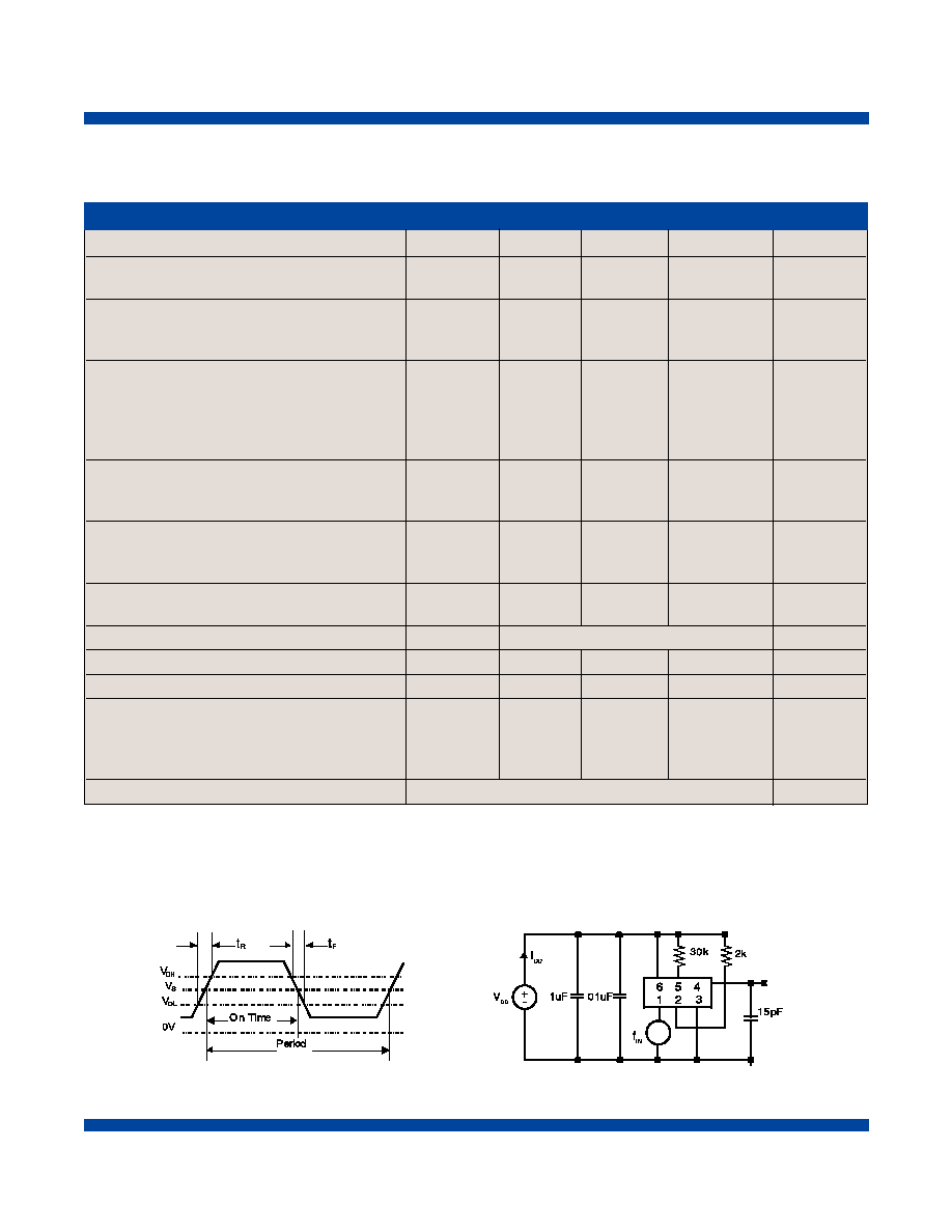
Figure 2. Output Waveform
Figure 3. Output Test Conditions
(25 ±5°C)
1. A 0.1 µF low frequency tantalum bypass capacitor in parallel with a 0.01 µF high frequency ceramic capacitor is recommended.
2. Figure 2 defines the waveform parameters. Figure 3 illustrates the standard test conditions under which these parameters are
specified and tested.
3. Duty cycle is defined as (on time period), with VS = VDD/2, per Figure 2. Duty cycle is measured with a 15pf load per Figure 3.
4. Other frequencies may be available, please contact factory.
Output Frequency
4
f
0
0.100
77.76
MHz
Supply Voltage
1
V
DD
3.0
3.3
3.6
V
V
DD
4.5
5.0
5.5
V
Supply Current @ 19.44MHz
I
DD
15
20
mA
48.408MHz
I
DD
25
30
mA
77.760MHz
I
DD
35
40
mA
Input
Input Low Level Voltage
V
IL
0.3* V
DD
V
Input High Level Voltage
V
IH
0.7*V
DD
V
Frequency
f
IN
1k
77.76M
Hz
Pulse Width
6
ns
Output
2
Output High Level Voltage
V
OH
0.9*V
DD
V
Output Low Level Voltage
V
OL
0.1*V
DD
V
Transition times
2
Rise Time
t
R
1.8
3.0
ns
Fall Time
t
F
1.8
3.0
ns
Duty Cycle
3
60MHz
D
45
55
%
>60MHz
40
60
Absolute Pull Range
APR
See Part Numbering
ppm
Leakage Current of Input
I
C
-1
1
µA
Loop Bandwidth (-3 dB), 8kHz input
BW
10
Hz
Jitter
(Application: 8 kHz to 77.760 MHz translation)
rms
4.7
ps
peak/peak
44
ps
peak/peak
0.003
UI
Size
14mm x 9mm x 4.5 mm
Parameter
Symbol
Minimum
Typical
Maximum
Units
FX-500 Low Jitter Frequency Translator
Vectron International ·
267 Lowell Road, Hudson, NH 03051 · Tel: 1-88-VECTRON-1 · Web: www.vectron.com
3
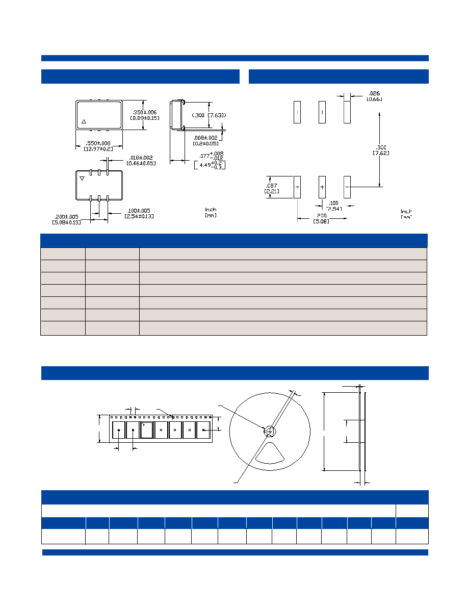
Outline Diagram
Pad Layout
Tape and Reel
A
E
C
D
B
G
F
J
L
I
K
H
Tape Dimensions
Reel Dimensions
# Per Reel
Product A
B C D E
F
G
H
I
J
K
L
FX-500
24 11.5 1.5
4
12
1.78
21
13 100 5
25 330
200
Tape and Reel Dimensions (mm)
FX-5
FX-500
00-LAC-GNK
-LAC-GNK
8K000/77M76
8K000/77M760
VI 142
VI 142
1
4
3
6
2
5
Pin #
Symbol
Function
1
f
IN
Input Frequency
2
Tri-state
1
Logic Low = Output Disable / Logic High = Output Enabled
3
GND
Case and Electrical Ground
4
F
o
Output Frequency
5
LD
2
Lock Detect
6
V
DD
Power Supply Voltage (3.3 V ± 0.3 or 5.0 V ± 0.5)
Pin Out
1. Tristate is driven to logic high or logic low; there is no internal pull up or pull down resistor.
2. LD is an open collector output requiring a 30k ohm pullup resistor to V
DD
. LD output is logic high under locked condition, logic
low for no input at f
IN
, and for "out-of-lock" condition LD transitions between logic low and logic high at the phase detector frequency.
4
FX-500 Low Jitter Frequency Translator
Vectron International ·
267 Lowell Road, Hudson, NH 03051 · Tel: 1-88-VECTRON-1 · Web: www.vectron.com
Absolute Maximum Ratings
Power Supply
V
DD
7
Vdc
Storage Temperature
Tstorage
-55/125
°C
Stresses in excess of the absolute maximum ratings can permanently damage the device. Functional operation is
not implied at these or any other conditions in excess of conditions represented in the operational sections of this
data sheet. Exposure to absolute maximum ratings for extended periods may adversely affect device reliability.
Parameter
Symbol
Ratings
Unit
Mechanical Shock
1000V
MIL-STD-883, Method 3015
Mechanical Vibration
1000V
JESD22-C101
Model
Minimum
Conditions
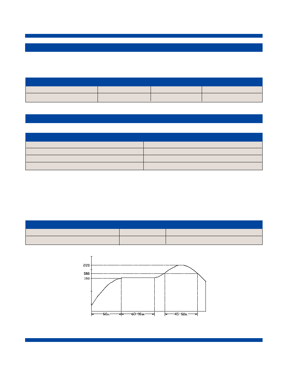
Figure 6. Suggested Reflow Profile
Absolute Maximum Ratings
Mechanical Shock
MIL-STD-883 Method 2002/Test A
Mechanical Vibration
MIL-STD-883 Method 2007/Test A
Lead Solderability
MIL-STD-883 Method 2003
Gross and Fine Leak
MIL-STD-883 Method 1014
Parameter
Conditions
Reliability
Handling Precautions
Although ESD protection circuitry has been designed into this device, proper precautions should be taken when
handling and mounting. VI employs a Human Body Model and a charged device model for ESD-susceptibility
testing and design protection evaluation. ESD thresholds are dependent on the circuit parameters used to define
the model. Although no industry wide standard has been adopted for the CDM, a standard HBM of resistance =
1500 and capacitance = 100pf is widely used and therefore can be used for comparison purposes.
ESD Ratings
FX-500 Low Jitter Frequency Translator
5
Vectron International ·
267 Lowell Road, Hudson, NH 03051 · Tel: 1-88-VECTRON-1 · Web: www.vectron.com
Ordering Information
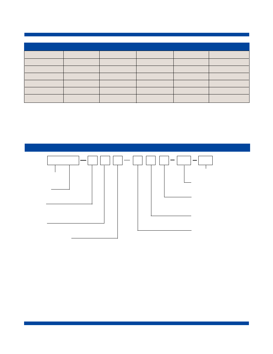
EXAMPLE: FX-500-LAC-GNK-A3-K2
FX-500, 3.3V, CMOS output, 0 to 70C operating temperature,
±50 ppm APR, 40/60 % duty cycle with an 8kHz input and 77.760MHz output
FX-500
X X X
X
X
X
XX
Input Frequency
(A1-K2 from table)
Duty Cycle
J = 45/55
K = 40/60
Other
N = n/a
Absolute Pull Range
G = ±50 ppm
N = ±80 ppm
H = ±100 ppm
Product Family
FX=Freq. Translator
Package
500: 14.0 x 9.0 x 4.5 mm
Input
K: 5.0V ±o.5 Vdc
L: 3.3V ±0.3 Vdc
Output
A: CMOS
Temperature Range
C: 0 to 70°C
F: -40 to 85°C
MHz
Output Frequency
(B2-K2 from table)
XX
1.000 kHz A1
4.000 kHz A2
8.000 kHz A3
16.000 kHz A4
64.000 kHz A5
1.024 MHz B2
1.544 MHz B3
2.048 MHz B4
3.088 MHz B6
4.096 MHz B5
6.480 MHz C2
8.192 MHz C3
10.000 MHz C4
12.352 MHz D1
13.000 MHz D3
15.000 MHz D4
16.384 MHz D5
18.432 MHz D7
19.440 MHz D6
20.000 MHz E2
20.480 MHz E4
24.576 MHz E6
24.704 MHz E7
26.000 MHz F3
27.000 MHz F4
30.720 MHz H1
32.000 MHz H2
32.768 MHz H3
34.368 MHz H6
37.056 MHz H4
38.880 MHz H5
40.960 MHz J1
44.736 MHz J3
49.152 MHz J7
51.840 MHz J4
61.440 MHz J5
62.208 MHz J8
62.500 MHz J9
65.536 MHz J6
74.152 MHz K1
74.250 MHz K7
77.760 MHz K2
Standard Frequencies
Note 1: Other frequencies are available upon request, please contact VI for details
SS is code for non-standard frequencies, list the frequency after the part number.
Note 2: Not all combinations are possible.
Note 3: Output frequency must be equal to or greater than the input frequency. The ratio of f
O
/f
IN
must be an Integer.
Also, the output frequency must be equal to or greater than 100 kHz.