 | ÐлекÑÑоннÑй компоненÑ: FX-700 | СкаÑаÑÑ:  PDF PDF  ZIP ZIP |
Äîêóìåíòàöèÿ è îïèñàíèÿ www.docs.chipfind.ru
Product Data Sheet
FX-700
Low Jitter Frequency Translator
Features
· 5.0 x 7.5 mm, Hermetically sealed SMD package
· Frequency Translation to 77.760 MHz
· 3.3 Volt or 5.0 Volt Supply
· Tri-State Output allows board test
· Lock Detect
· Commercial or Industrial Temp. Range
· CMOS Output
· Absolute Pull Range Performance to +/-100 ppm
· Capable of locking to an 8 kHz pulse/BITS clock
Applications
· Frequency Translation, Clock Smoothing
· Telecom - SONET/SDH/ATM
· Datacom DSLAM, DSLAR, Access Nodes
· Base Station GSM, CDMA
· Cable Modem Head End
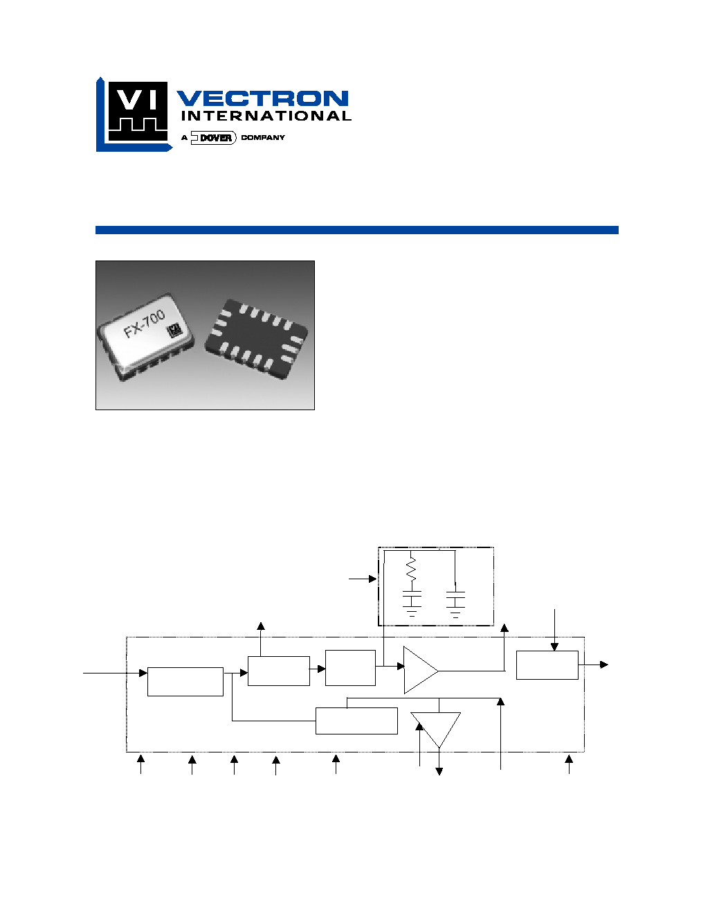
C1 Charge
Pump Out
(5)
V
COUT
(3)
GND
B
(9)
V
DB
(11)
V
DD
(1)
GND
(7)
VCXO
IN
(12)
F
OUT
(10)
VCXO
OUT
(13)
Buffer
Buffer
LD
(8)
Tri-State
(4)
Input Frequency
Divider (1-64)
Output Frequency
Divider (1-16384)
FX-700
Phase/Freq.
Detector
VCXO
Charge
Pump
F
IN
(6)
V
CIN
(16)
R2
C2
C1
External Loop Filter
V
DA
(2)
V
DO
(14)
Figure 1. FX-700 Block Diagram
Description
The FX-700 is a crystal-based frequency translator
used in communications applications where low jit-
ter is paramount.
Performance advantages include superior jitter
performance, high output frequencies and small
package size. Advanced custom ASIC technology
results in a highly robust, reliable and predictable
device. The device is packaged in a 16 pad ceram-
ic package with a hermetic seam welded lid.
8983_VECTRON 06/17/02 12:13 PM Page 1
FX-700 Low Jitter Frequency Translator
Performance Characteristics
Vectron International · 267 Lowell Road, Hudson, NH 03051 · Tel: 1-88-VECTRON-1 · Web: www.vectron.com
2
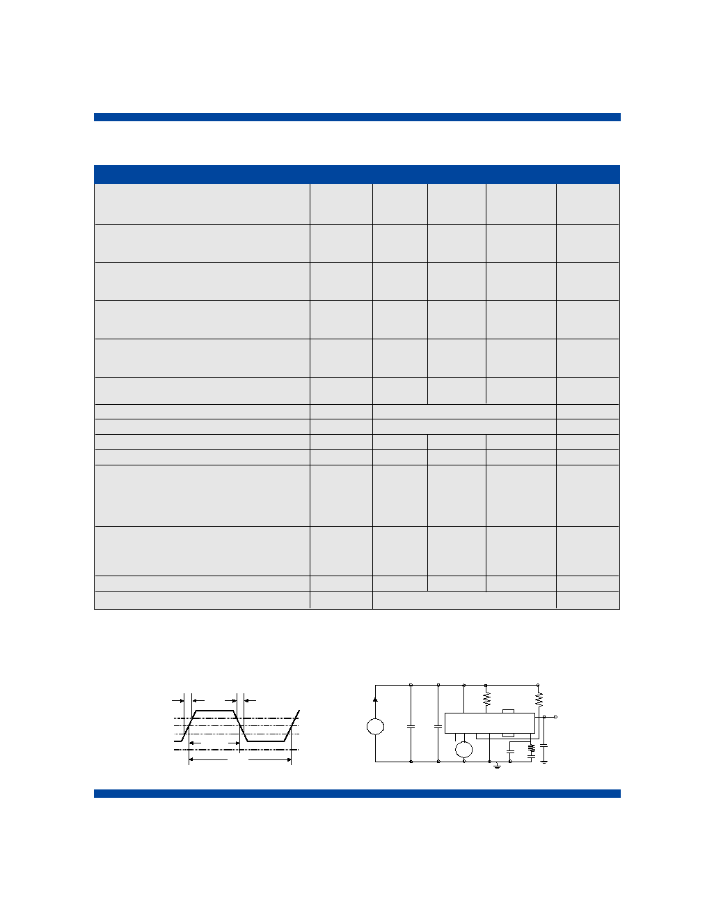
Figure 2. Output Waveform
Figure 3. Output Test Conditions (25
±
5
°
C)
+
-
f
IN
10
7,9
.
1uF
.01uF
15pF
8
4
2,14,11,1
6
I
DD
V
DD
30k
2k
15
n/c
13,12
3,16
5
C1
C2
R2
80
%
Vs
20
%
t
F
t
R
Period
On Time
1. A 0.01uF high frequency ceramic capacitor in parallel with a 0.1uF low frequency tantalum bypass capacitor is recommended
2. Figure 2 defines the waveform parameters. Figure 3 illustrates the standard test conditions under which these parameters are tested and specified
3. Duty Cycle is defined as (on time/period) with Vs = Vdd/2 per Figure 2. Duty Cycle is measured with a 15pf load per Figure 3.
4. Other frequencies may be available, please contact factory.
5. Combined Current From V
DD
, V
DO
, V
DA
, and V
DB
6. Typical jitter for 8 kHz to 77.760 MHz translation (no offset bandwidth).
Electrical Performance
Output Frequency
4
Output (3.3 V)
fo
0.100
77.760
MHz
Output (5.0 V)
fo
0.100
77.760
MHz
Supply Voltage
1
(V
DD
,V
DB
,V
DA
,V
DO
)
+5.0
V
DD
4.5
5.0
5.5
V
+3.3
V
DD
2.97
3.3
3.63
V
Supply Current
5
@19.440 MHz
I
DD
15
20
mA
49.152 MHz
I
DD
25
30
mA
77.760 MHz
I
DD
35
40
mA
Output
2
Output High
V
OH
0.9*Vdd
V
Output Low
V
OL
0.1*Vdd
V
Transition Times
2
Rise Time
t
R
1.8
3.0
ns
Fall Time
t
F
1.8
3.0
ns
Duty Cycle
3
<60 MHz
D
45
50
55
%
60 MHz
40
50
60
%
Absolute Pull Range
APR
See Part Numbering
ppm
Operating Temperature:
0 to 70°C or -40 to 85°C
Test Conditions for APR (+5V option)
V
C
0.5
4.5
V
Test Conditions for APR (+3.3V option)
V
C
0.3
3.0
V
Input
Frequency f
IN
1 kHz
77.76 MHz
Pulse Width
6.0
ns
Low Logic Level
V
IL
0.3* Vdd
V
High Logic Level
V
IH
0.7* Vdd
V
Jitter, 8kHz to 77.760 MHz
6
rms
4.7
ps
peak/peak
44
ps
peak/peak
0.003
UI
Leakage Current of Input
IC
-1
+1
uA
Size
5.0mm x 7.5mm x 2.0mm
Parameter
Symbol
Minimum
Typical
Maximum
Units
8983_VECTRON 06/17/02 12:13 PM Page 2
FX-700 Low Jitter Frequency Translator
Vectron International · 267 Lowell Road, Hudson, NH 03051 · Tel: 1-88-VECTRON-1 · Web: www.vectron.com
3
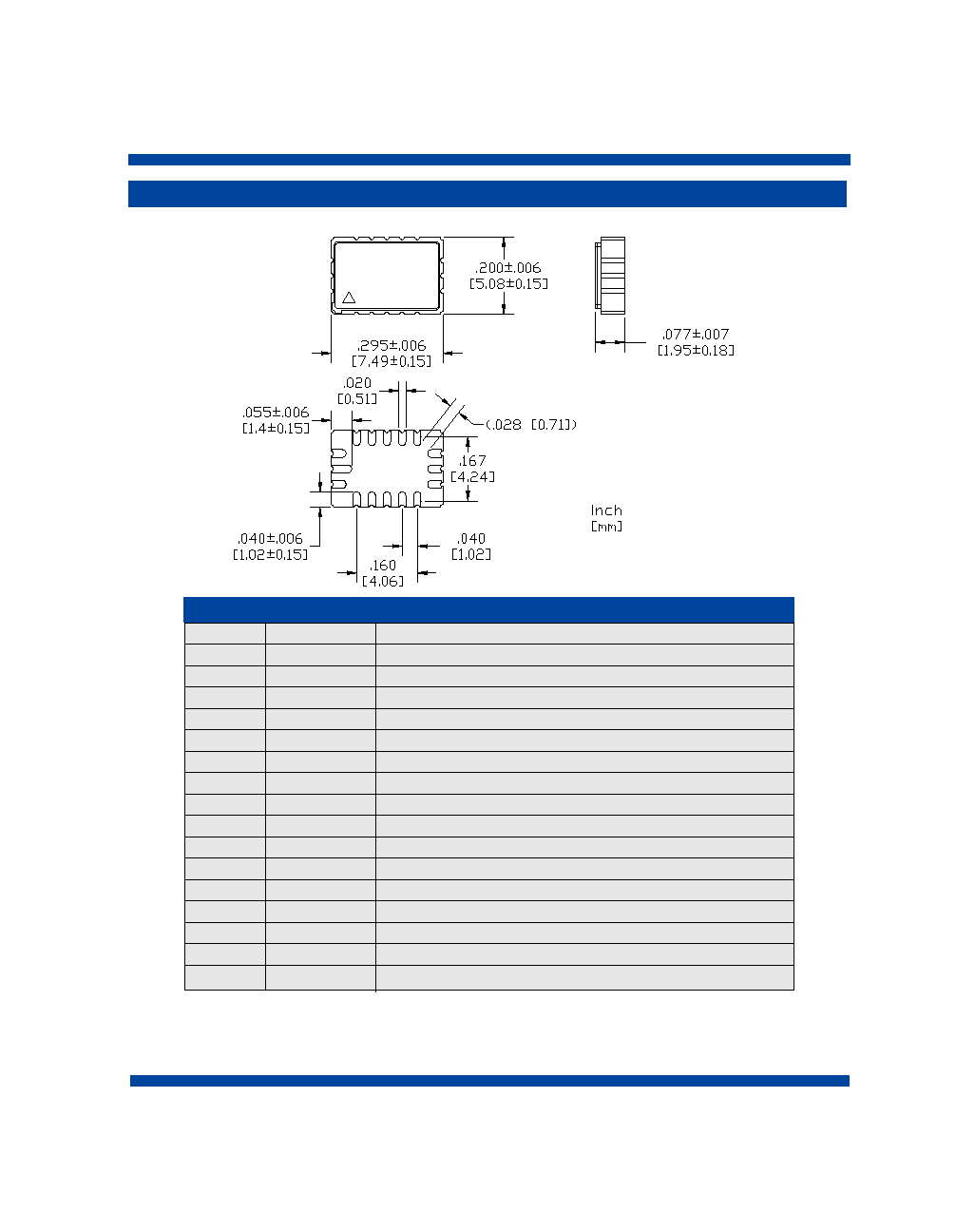
Outline Diagram
1
9
5
6
8
13
14
16
FLACGNK
A3/K2
VI YWW
2 3 4
7
10
11
12
15
Pin #
Symbol
Function
1
V
DD
Digital PLL Supply (3.3 V +/- 10% or 5.0 V +/- 10%)
2 V
DA
Analog PLL Supply (3.3 V +/- 10% or 5.0 V +/- 10%)
3
V
COUT
Control Voltage
4
Tri-state
1
Logic Low = Output Disable / Logic High = Output Enabled
5
C1
Passive Loop Filter Node
6
F
IN
Input Frequency
7
GND
Cover and Electrical Ground
8
LD
2
Lock Detect
9
GND
B
Output Buffer Ground
10
F
OUT
Output Frequency
11
V
DB
Output Buffer Supply (3.3V +/-10% or 5.0V +/-10%)
12
VCXO
IN
VCXO Input
13
VCXO
OUT
VCXO Output
14
V
DO
VCXO Supply (3.3 V +/- 10% or 5.0 V +/- 10%)
15
N.C.
No Internal Connection Made
16
VC
IN
VCXO Control Voltage Input
Pin Out
1 Tri-state must be driven to a logic high or a logic low, there is no internal pull up or pull down resistor (tie pin to VDD for
PLL operation).
2 LD is an open collector output requiring a 30k ohm minimum pull-up resistor to VDD. LD output is logic high under
locked condition, logic low for no input at FIN, and for "out-of-lock" condition LD transitions between logic low and high
at the phase detector frequency.
8983_VECTRON 06/17/02 12:13 PM Page 3
FX-700 Low Jitter Frequency Translator
Vectron International · 267 Lowell Road, Hudson, NH 03051 · Tel: 1-88-VECTRON-1 · Web: www.vectron.com
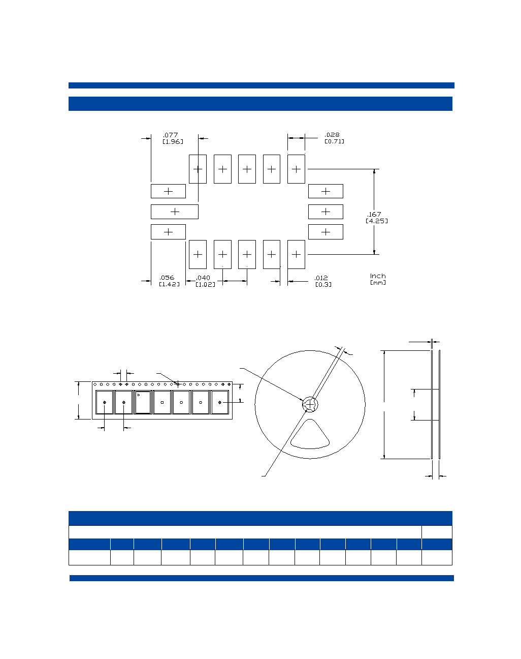
Solder Pad Layout
Tape Dimensions
Reel Dimensions
# Per Reel
Product A
B C D E
F
G
H
I
J
K
L
FX-700
16 7.5 1.5
4
8
1.5
20.2
13 50 6
16.4
178
500
Tape and Reel Dimensions (mm)
A
E
C
D
B
G
F
J
L
I
K
H
4
8983_VECTRON 06/17/02 12:13 PM Page 4
5
FX-700 Low Jitter Frequency Translator
Vectron International · 267 Lowell Road, Hudson, NH 03051 · Tel: 1-88-VECTRON-1 · Web: www.vectron.com
Absolute Maximum Ratings
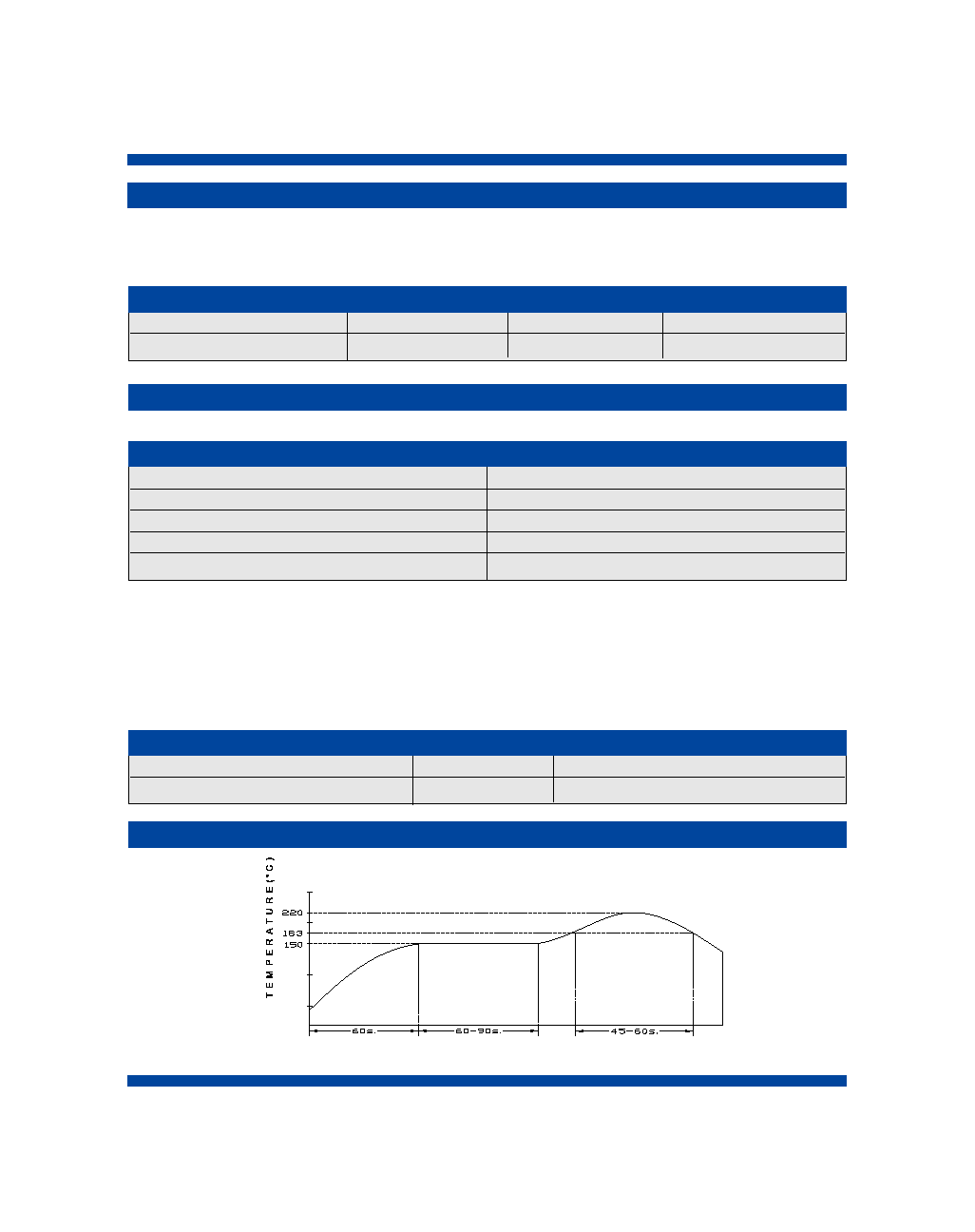
Recommended Solder Reflow Profile
Power Supply
V
DD
7
Vdc
Storage Temperature
Tstorage
-55/125
°C
Stresses in excess of the absolute maximum ratings can permanently damage the device. Functional operation is
not implied at these or any other conditions in excess of conditions represented in the operational sections of this
data sheet. Exposure to absolute maximum ratings for extended periods may adversely affect device reliability.
Parameter
Symbol
Ratings
Unit
Human Body Model
1500
MIL-STD-883, Method 3015
Charged Device Model
1000
JESD 22-C101
Model
Minimum
Conditions
Absolute Maximum Ratings
Mechanical Shock
MIL-STD-883 Method 2002
Mechanical Vibration
MIL-STD-883 Method 2007
Solderability
MIL-STD-883 Method 2003
Gross and Fine Leak
MIL-STD-883 Method 1014
Resistance to Solvents
MIL-STD-883 Method 2016
Parameter
Conditions
Reliability
Handling Precautions
Although ESD protection circuitrry has been designed into the the FX-700, proper precautions should be taken
when handling and mounting. VI employs a human body model and a charged-device model (CDM) for ESD sus-
ceptibility testing and design protection evaluation. ESD thresholds are dependent on the circuit parameters used
to define the model. Although no industry wide standard has been adopted for the CDM, a standard HBM of resist-
ance=1.5Kohms and capacitance = 100pF is widely used and Therefore can be used for comparison purposes.
ESD Ratings
Times(s)
8983_VECTRON 06/17/02 12:13 PM Page 5