Product Data Sheet
FX-700
Low Jitter Frequency Translator
Features
∑ 5.0 x 7.5 mm, Hermetically sealed SMD package
∑ Frequency Translation to 77.760 MHz
∑ 3.3 Volt or 5.0 Volt Supply
∑ Tri-State Output allows board test
∑ Lock Detect
∑ Commercial or Industrial Temp. Range
∑ CMOS Output
∑ Absolute Pull Range Performance to +/-100 ppm
∑ Capable of locking to an 8 kHz pulse/BITS clock
Applications
∑ Frequency Translation, Clock Smoothing
∑ Telecom - SONET/SDH/ATM
∑ Datacom ≠ DSLAM, DSLAR, Access Nodes
∑ Base Station ≠ GSM, CDMA
∑ Cable Modem Head End
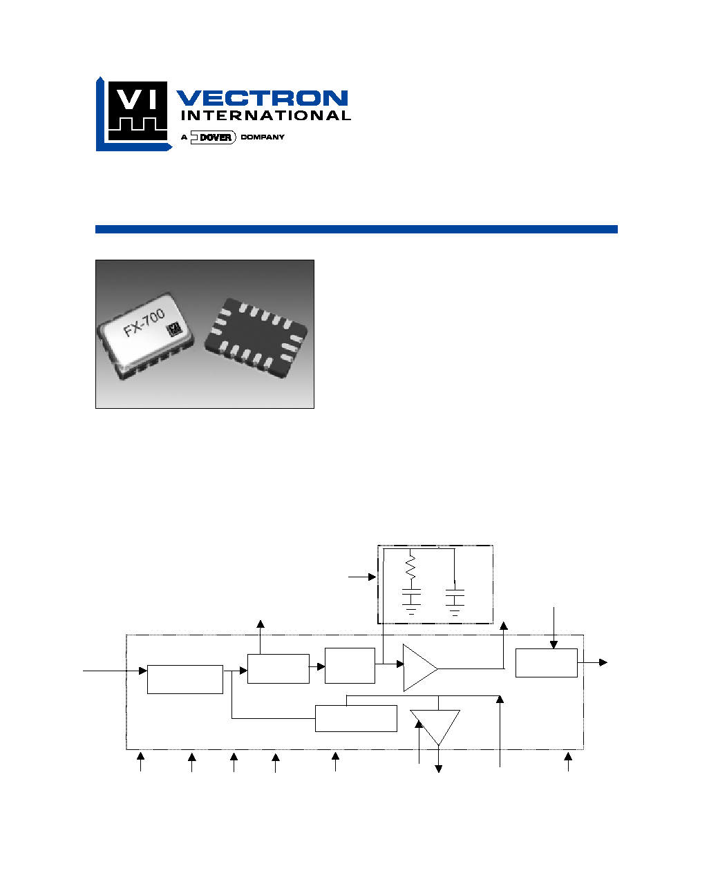
C1 Charge
Pump Out
(5)
V
COUT
(3)
GND
B
(9)
V
DB
(11)
V
DD
(1)
GND
(7)
VCXO
IN
(12)
F
OUT
(10)
VCXO
OUT
(13)
Buffer
Buffer
LD
(8)
Tri-State
(4)
Input Frequency
Divider (1-64)
Output Frequency
Divider (1-16384)
FX-700
Phase/Freq.
Detector
VCXO
Charge
Pump
F
IN
(6)
V
CIN
(16)
R2
C2
C1
External Loop Filter
V
DA
(2)
V
DO
(14)
Figure 1. FX-700 Block Diagram
Description
The FX-700 is a crystal-based frequency translator
used in communications applications where low jit-
ter is paramount.
Performance advantages include superior jitter
performance, high output frequencies and small
package size. Advanced custom ASIC technology
results in a highly robust, reliable and predictable
device. The device is packaged in a 16 pad ceram-
ic package with a hermetic seam welded lid.
8983_VECTRON 06/17/02 12:13 PM Page 1
FX-700 Low Jitter Frequency Translator
Performance Characteristics
Vectron International ∑ 267 Lowell Road, Hudson, NH 03051 ∑ Tel: 1-88-VECTRON-1 ∑ Web: www.vectron.com
2
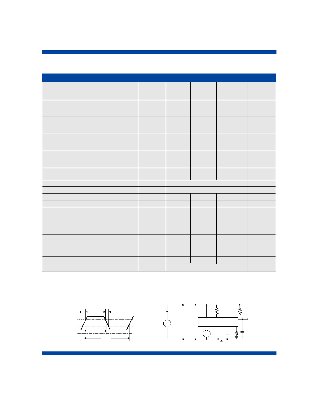
Figure 2. Output Waveform
Figure 3. Output Test Conditions (25
±
5
∞
C)
+
-
f
IN
10
7,9
.
1uF
.01uF
15pF
8
4
2,14,11,1
6
I
DD
V
DD
30k
2k
15
n/c
13,12
3,16
5
C1
C2
R2
80
%
Vs
20
%
t
F
t
R
Period
On Time
1. A 0.01uF high frequency ceramic capacitor in parallel with a 0.1uF low frequency tantalum bypass capacitor is recommended
2. Figure 2 defines the waveform parameters. Figure 3 illustrates the standard test conditions under which these parameters are tested and specified
3. Duty Cycle is defined as (on time/period) with Vs = Vdd/2 per Figure 2. Duty Cycle is measured with a 15pf load per Figure 3.
4. Other frequencies may be available, please contact factory.
5. Combined Current From V
DD
, V
DO
, V
DA
, and V
DB
6. Typical jitter for 8 kHz to 77.760 MHz translation (no offset bandwidth).
Electrical Performance
Output Frequency
4
Output (3.3 V)
fo
0.100
77.760
MHz
Output (5.0 V)
fo
0.100
77.760
MHz
Supply Voltage
1
(V
DD
,V
DB
,V
DA
,V
DO
)
+5.0
V
DD
4.5
5.0
5.5
V
+3.3
V
DD
2.97
3.3
3.63
V
Supply Current
5
@19.440 MHz
I
DD
15
20
mA
49.152 MHz
I
DD
25
30
mA
77.760 MHz
I
DD
35
40
mA
Output
2
Output High
V
OH
0.9*Vdd
V
Output Low
V
OL
0.1*Vdd
V
Transition Times
2
Rise Time
t
R
1.8
3.0
ns
Fall Time
t
F
1.8
3.0
ns
Duty Cycle
3
<60 MHz
D
45
50
55
%
60 MHz
40
50
60
%
Absolute Pull Range
APR
See Part Numbering
ppm
Operating Temperature:
0 to 70∞C or -40 to 85∞C
Test Conditions for APR (+5V option)
V
C
0.5
4.5
V
Test Conditions for APR (+3.3V option)
V
C
0.3
3.0
V
Input
Frequency f
IN
1 kHz
77.76 MHz
Pulse Width
6.0
ns
Low Logic Level
V
IL
0.3* Vdd
V
High Logic Level
V
IH
0.7* Vdd
V
Jitter, 8kHz to 77.760 MHz
6
rms
4.7
ps
peak/peak
44
ps
peak/peak
0.003
UI
Leakage Current of Input
IC
-1
+1
uA
Size
5.0mm x 7.5mm x 2.0mm
Parameter
Symbol
Minimum
Typical
Maximum
Units
8983_VECTRON 06/17/02 12:13 PM Page 2
FX-700 Low Jitter Frequency Translator
Vectron International ∑ 267 Lowell Road, Hudson, NH 03051 ∑ Tel: 1-88-VECTRON-1 ∑ Web: www.vectron.com
3
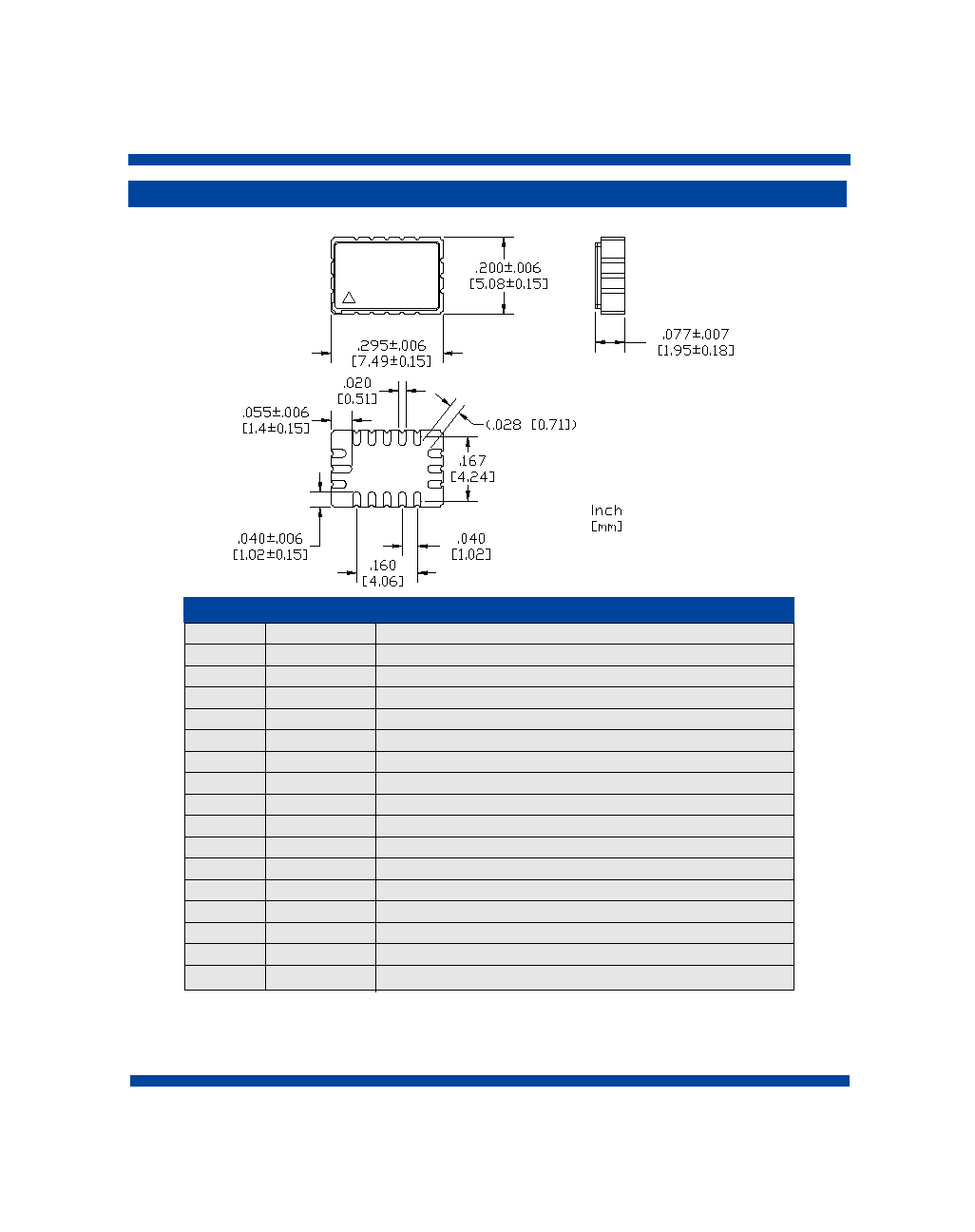
Outline Diagram
1
9
5
6
8
13
14
16
FLACGNK
A3/K2
VI YWW
2 3 4
7
10
11
12
15
Pin #
Symbol
Function
1
V
DD
Digital PLL Supply (3.3 V +/- 10% or 5.0 V +/- 10%)
2 V
DA
Analog PLL Supply (3.3 V +/- 10% or 5.0 V +/- 10%)
3
V
COUT
Control Voltage
4
Tri-state
1
Logic Low = Output Disable / Logic High = Output Enabled
5
C1
Passive Loop Filter Node
6
F
IN
Input Frequency
7
GND
Cover and Electrical Ground
8
LD
2
Lock Detect
9
GND
B
Output Buffer Ground
10
F
OUT
Output Frequency
11
V
DB
Output Buffer Supply (3.3V +/-10% or 5.0V +/-10%)
12
VCXO
IN
VCXO Input
13
VCXO
OUT
VCXO Output
14
V
DO
VCXO Supply (3.3 V +/- 10% or 5.0 V +/- 10%)
15
N.C.
No Internal Connection Made
16
VC
IN
VCXO Control Voltage Input
Pin Out
1 Tri-state must be driven to a logic high or a logic low, there is no internal pull up or pull down resistor (tie pin to VDD for
PLL operation).
2 LD is an open collector output requiring a 30k ohm minimum pull-up resistor to VDD. LD output is logic high under
locked condition, logic low for no input at FIN, and for "out-of-lock" condition LD transitions between logic low and high
at the phase detector frequency.
8983_VECTRON 06/17/02 12:13 PM Page 3
FX-700 Low Jitter Frequency Translator
Vectron International ∑ 267 Lowell Road, Hudson, NH 03051 ∑ Tel: 1-88-VECTRON-1 ∑ Web: www.vectron.com
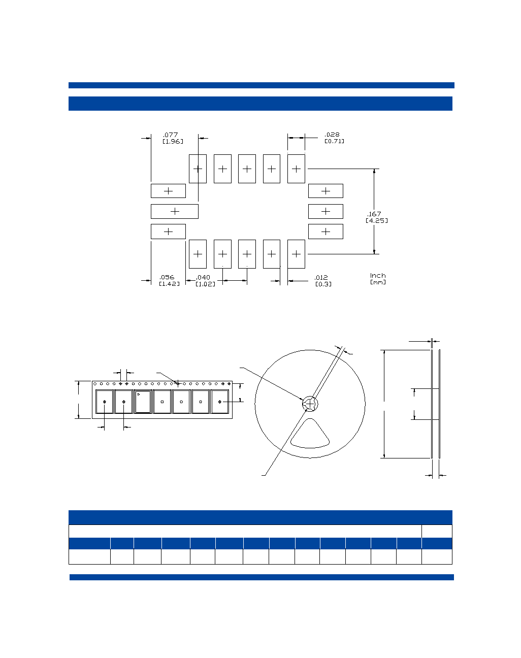
Solder Pad Layout
Tape Dimensions
Reel Dimensions
# Per Reel
Product A
B C D E
F
G
H
I
J
K
L
FX-700
16 7.5 1.5
4
8
1.5
20.2
13 50 6
16.4
178
500
Tape and Reel Dimensions (mm)
A
E
C
D
B
G
F
J
L
I
K
H
4
8983_VECTRON 06/17/02 12:13 PM Page 4
5
FX-700 Low Jitter Frequency Translator
Vectron International ∑ 267 Lowell Road, Hudson, NH 03051 ∑ Tel: 1-88-VECTRON-1 ∑ Web: www.vectron.com
Absolute Maximum Ratings
Recommended Solder Reflow Profile
Power Supply
V
DD
7
Vdc
Storage Temperature
Tstorage
-55/125
∞C
Stresses in excess of the absolute maximum ratings can permanently damage the device. Functional operation is
not implied at these or any other conditions in excess of conditions represented in the operational sections of this
data sheet. Exposure to absolute maximum ratings for extended periods may adversely affect device reliability.
Parameter
Symbol
Ratings
Unit
Human Body Model
1500
MIL-STD-883, Method 3015
Charged Device Model
1000
JESD 22-C101
Model
Minimum
Conditions
Absolute Maximum Ratings
Mechanical Shock
MIL-STD-883 Method 2002
Mechanical Vibration
MIL-STD-883 Method 2007
Solderability
MIL-STD-883 Method 2003
Gross and Fine Leak
MIL-STD-883 Method 1014
Resistance to Solvents
MIL-STD-883 Method 2016
Parameter
Conditions
Reliability
Handling Precautions
Although ESD protection circuitrry has been designed into the the FX-700, proper precautions should be taken
when handling and mounting. VI employs a human body model and a charged-device model (CDM) for ESD sus-
ceptibility testing and design protection evaluation. ESD thresholds are dependent on the circuit parameters used
to define the model. Although no industry wide standard has been adopted for the CDM, a standard HBM of resist-
ance=1.5Kohms and capacitance = 100pF is widely used and Therefore can be used for comparison purposes.
ESD Ratings
Times(s)
8983_VECTRON 06/17/02 12:13 PM Page 5

6
FX-700 Low Jitter Frequency Translator
Vectron International ∑ 267 Lowell Road, Hudson, NH 03051 ∑ Tel: 1-88-VECTRON-1 ∑ Web: www.vectron.com
FX-700 Theory of Operation
The FX-700 includes an integrated phase
detector, current mode charge pump,
programmable frequency dividers and VCXO.
The FX-700 will translate an input frequency
such as 8 kHz, 1.544 MHz or 19.440 MHz to
a specific output frequency which is an integer
multiple (1-16384) of the input frequency and
less than or equal to 77.760 MHz. For clock
smoothing applications, the input frequency is
typically internally divided down by a factor of
64 (2N where N = 6) by the input frequency
divider and this frequency becomes an input
to the phase detector. The integrated
frequency dividers (factory programmed)
and crystal based VCXO allows for a large
range of possible frequency translations and
clock smoothing applications.
The FX-700's PLL is a feedback system which
forces the output frequency to lock in both
phase and frequency to the input frequency.
While there will be some phase error, theory
states there is no frequency error. The loop
filter design will dictate many key parameters
such as jitter reduction, stability, lock range
and acquisition time. The external second
order passive loop filter is a complex imped-
ance in parallel with the input capacitance of
the VCXO. The loop filter converts the charge
pump output into the VCXO's control voltage.
VI's loop filter design methodology involves
the calculation of the open loop gain band-
width and corresponding phase margin to
determine the optimal component values that
ensure high loop stability and acceptable lock
in time. As a rule of thumb, the VCXO gain is
typically 100 ppm/volt and the charge pump
current is typically 32 uA.
VI's Applications Engineering staff can provide
the external loop filter component values
required to meet specific system requirements
and application
8983_VECTRON 06/17/02 12:13 PM Page 6

FX-700 Low Jitter Frequency Translator
7
Vectron International ∑ 267 Lowell Road, Hudson, NH 03051 ∑ Tel: 1-88-VECTRON-1 ∑ Web: www.vectron.com
Ordering Information
EXAMPLE: FX-700-LAC-GNK-A3-K2
FX-700, 3.3V, CMOS output, 0 to 70C∞ operating temperature,
±50 ppm APR, 40/60 % duty cycle with an 8kHz input and 77.760MHz output
FX-700
X X X
X X X
XX
Input Frequency
(A1-K2 from table)
Duty Cycle
J = 45/55
K = 40/60
Other
N = n/a
Absolute Pull Range
G = ±50 ppm
N = ±80 ppm
H = ±100 ppm
Product Family
FX=Freq. Translator
Package
700: 5.0 x 7.5 x 2.0 mm
Input
K: 5.0V ±0.5 Vdc
L: 3.3V ±0.3 Vdc
Output
A: CMOS
Temperature Range
C: 0 to 70∞C
F: -40 to 85∞C
MHz
Output Frequency
(B2-K2 from table)
XX
1.000 KHz
A1
4.000 KHz
A2
8.000 KHz
A3
16.000 KHz
A4
64.000 KHz
A5
1.024 MHz
B2
1.544 MHz
B3
2.048 MHz
B4
3.088 MHz
B6
4.096 MHz
B5
6.480 MHz
C2
8.192 MHz
C3
10.000 MHz
C4
12.352 MHz
D1
13.000 MHz
D3
15.000 MHz
D4
16.384 MHz
D5
18.432 MHz
D7
19.440 MHz
D6
20.000 MHz
E2
20.480 MHz
E4
24.576 MHz
E6
24.704 MHz
E7
26.000 MHz
F3
27.000 MHz
F4
30.720 MHz
H1
32.000 MHz
H2
32.768 MHz
H3
34.368 MHz
H6
37.056 MHz
H4
38.880 MHz
H5
40.960 MHz
J1
44.736 MHz
J3
49.152 MHz
J7
51.840 MHz
J4
61.440 MHz
J5
62.208 MHz
J8
62.500 MHz
J9
65.536 MHz
J6
74.152 MHz
K1
74.250 MHz
K7
77.760 MHz
K2
Standard Frequencies
Note 1: Other frequencies are available upon request, please contact VI for details
SS is code for non-standard frequencies, list the frequency after the part number.
Note 2: Not all combinations are possible.
Note 3: The output frequency must be equal to or greater than the input frequency.
Note 4: The output frequency divided by the input frequency (F
OUT
/F
IN
) must be an integer.
Note 5: The output frequency must also be equal to or greater than 100 kHz.
8983_VECTRON 06/17/02 12:13 PM Page 7
USA: Vectron International ∑ 267 Lowell Road, Hudson, NH 03051 . . . Tel: 1-88-VECTRON-1 ∑ Fax: 1-888-FAX-VECTRON
EUROPE: . . . . . . . . . . . . . . . . . . . . . . . . . . . . . . . . . . . . . . . . . . . . . . . . . Tel: 49 (0) 3328 4784 17 * Fax: 49 (0) 3328 4784 30
ASIA:. . . . . . . . . . . . . . . . . . . . . . . . . . . . . . . . . . . . . . . . . . . . . . . . . . . . . Tel: +86 21 28909740 / 41 / 42 Fax: +86 21 28909240 / 28909999
Vectron International reserves the right to make changes to the product(s) and/or information contained herein without notice.
No liability is assumed as a result of their use or application. No rights under any patent accompany the sale of any such product(s) or information.
©2001, Vectron International. Rev.21Jun02
www.vectron.com
For additional information please contact:
FX-700 Low Jitter Frequency Translator
8983_VECTRON 06/17/02 12:13 PM Page 8