 | –≠–ª–µ–∫—Ç—Ä–æ–Ω–Ω—ã–π –∫–æ–º–ø–æ–Ω–µ–Ω—Ç: JCLFNCKTN | –°–∫–∞—á–∞—Ç—å:  PDF PDF  ZIP ZIP |
Product Data Sheet
J-Type
Voltage Controlled Crystal Oscillator
Features
∑ Output Frequencies from 1.024 MHz to 170.000 MHz
∑ +3.3 or +5.0 volt options
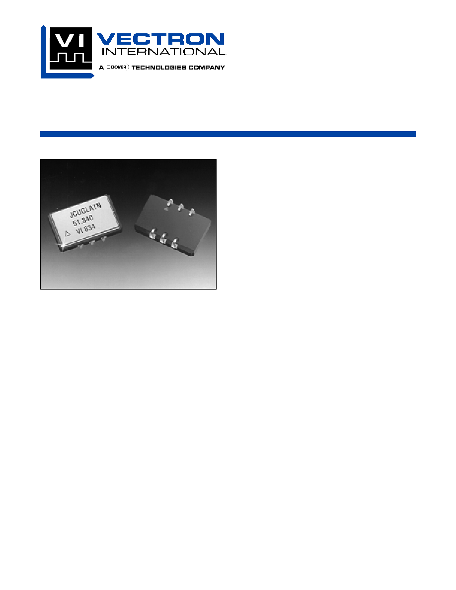
∑ Small 14mm x 9mm J-type Package
∑ CMOS or PECL Outputs
∑ Low phase noise and custom options
∑ 0/70∞ C or ≠40/85∞ C operating temperature
∑ Tri-State output (CMOS) Enable/Disable (PECL)
Applications
∑ Clock Smoothing
∑ Frequency Translation
∑ SONET, SDH, ATM, DSLAM, ADM
Description
The J-type voltage controlled crystal oscillator incorpo-
rates VI's advanced VCXO performance capabilities
while adhering to a package footprint compatible with
the industry-common J-lead package.
The J-type VCXO is a quartz stabilized square wave
generator with either a CMOS output for driving
CMOS/TTL loads or a PECL output. The device is pack-
aged in a 6 pin J-lead ceramic package and is hermeti-
cally sealed with a grounded conductive lid.
J-Type Voltage Controlled Crystal Oscillator
Vectron International ∑
267 Lowell Road, Hudson, NH 03051 ∑ Tel: 1-88-VECTRON-1 ∑ Fax: 1-888-FAX-VECTRON
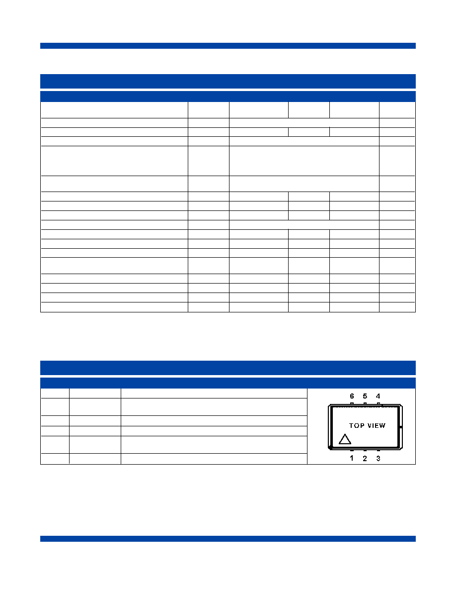
1
Vc VCXO
Control
Voltage.
2
Tri-State
1
TTL logic low disables output
TTL logic high, or no connect, enables output
3
GND
Case and electrical ground.
4
Output
VCXO Output
5
CMOS/TTL
TTL logic low optimizes symmetry for CMOS
select
1,2
TTL logic high, or NC, optimizes symmetry for TTL.
6
V
CC
Power Supply Voltage (5.0 V or 3.3V ±10%)
Pin Out Information for the CMOS output option
Electrical Performance @ 25∞C for the CMOS output option
CMOS Output Option
1. Standard option. Tri-State can be connected to pin 5 and CMOS/TTL select would be on pin 2.
2. Output is HCMOS. For frequencies >12MHz, this option optimizes symmetry for either CMOS or TTL thresholds. Ground this pin for fre-
quencies < 12MHz.
Supply Voltage
1
, +5 volt option
4.5
5.0
5.5
Vdc
+3.3 volt option
3.0
3.3
3.6
Vdc
Supply Current
10mA + 0.25mA per MHz, typical
Center Frequency, see ordering information
F
N
1.024
77.760
MHz
Operating Temperature, see ordering info
T
OP
0/70, -40/85
∞C
Absolute Pull Range over the operating tempera-
APR
±50 to ±100
ppm
ture range, aging and power supply Vc=0.5 to
4.5 at 5V supply or 0.3 to 3.0 V at 3.3V supply
see ordering information for options
Gain Transfer
K
V
Positive
(Frequency vs. Control Voltage)
Output Level High
2
V
OH
0.8*Vcc
-
V
Output Level Low
2
V
OL
-
0.1*Vcc
V
Output Rise/Fall Time
2
t
R
/ t
F
5
ns
Duty Cycle
3
, see ordering info
SYM
45/55 or 40/60
%
Control Input Leakage
I
L
1
uA
Control Voltage Modulation Bandwidth
BW
-
10
-
kHz
RMS Jitter, Output=12.0-77.760 MHz
3
ps
RMS Jitter, Output =12.0-77.760 MHz.
<0.5
ps
Band =12.0 KHz - 20 MHz
Control Range
0
V
DD
Maximum Supply Voltage
7
V
Storage Temperature
T
S
-55
-
125
∞C
Soldering Temp./Time
T
LS
-
-
220/10
∞C/s
2
Parameter
Symbol
Minimum
Typical Maximum
Unit
1. Power supply bypass is required and a 0.1uF in parallel with a 0.01uF high frequency capacitor is recommended.
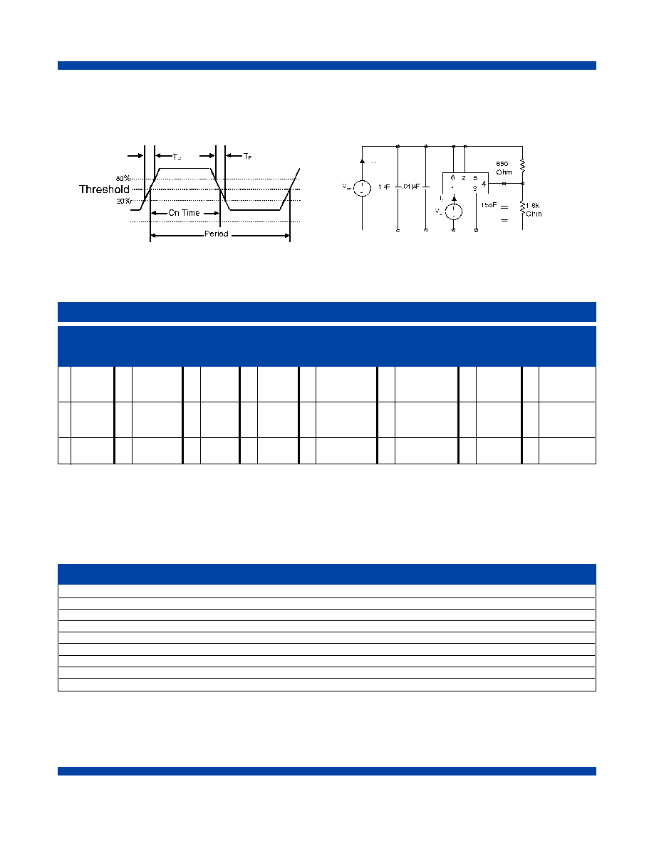
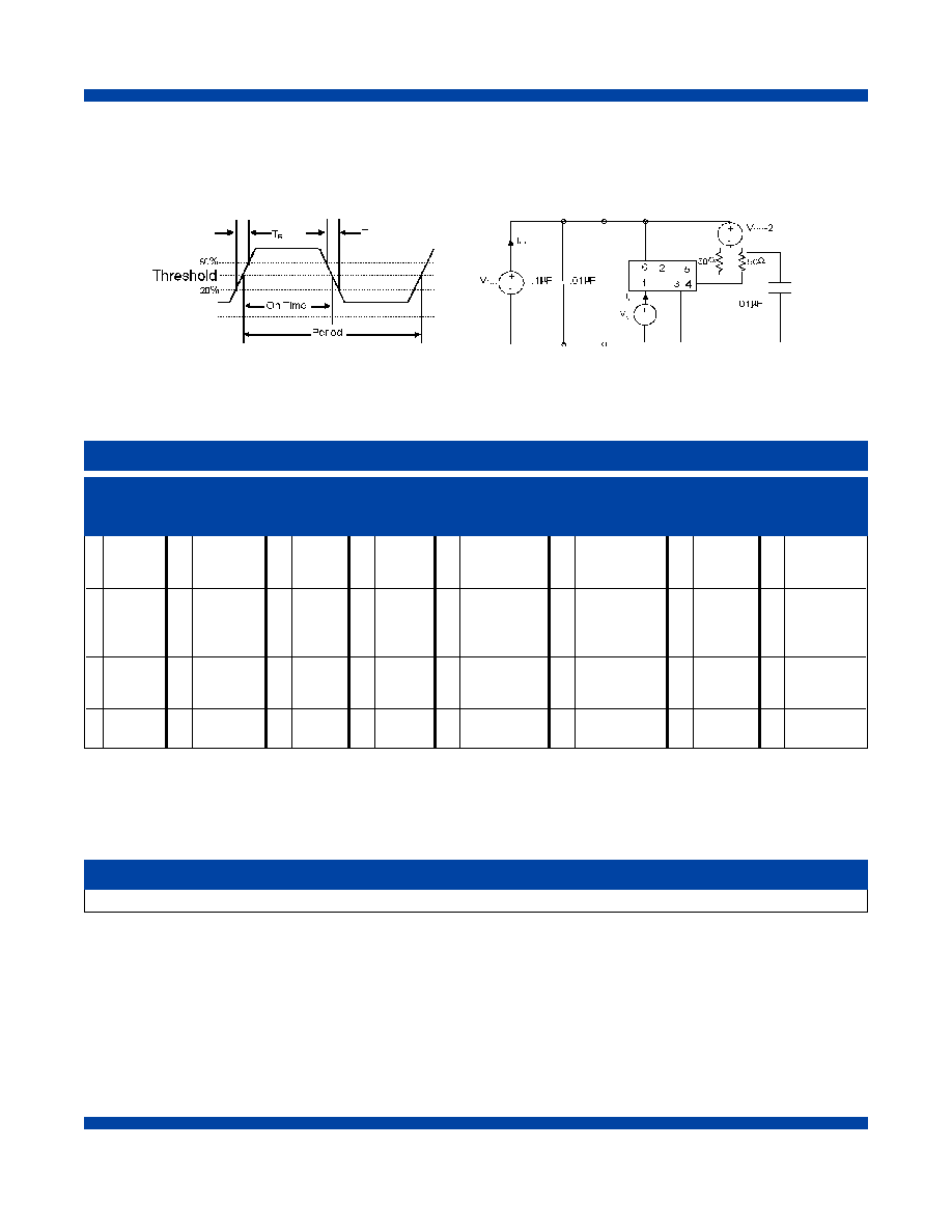
2. Figure 1 defines these parameters. Figure 2 illustrates the load used to test devices.
3. Duty cycle is defined as on-time versus period at 1.4 V for TTL, and 2.5 V for CMOS (5volt supply) and at 1.65 V for CMOS (3.3 volt operation)
Pin
Symbol
Function
J-Type Voltage Controlled Crystal Oscillator
Vectron International ∑
267 Lowell Road, Hudson, NH 03051 ∑ Tel: 1-88-VECTRON-1 ∑ Fax: 1-888-FAX-VECTRON
CMOS Output Option
3
Output Test Conditions (25±5∞C) for 5 volt devices.
For 3.3V use 15pF cap only, no resistors needed.
Threshold = 1.4 volts for TTL
and 50% for CMOS
Figure 1
Output Wave Form
Figure 2
Output Test Conditions
1.024
1.544
2.000
2.048
3.088
3.580
3.686
4.000
4.032
4.096
4.434
5.000
6.144
6.176
6.312
6.400
8.000
8.192
8.448
10.000
12.000
12.288
12.352
13.000
14.318
15.360
15.440
16.000
16.384
18.432
19.44
20.000
20.480
24.000
24.576
24.704
27.000
30.000
32.000
32.768
34.368
35.328
38.880
40.000
40.960
44.736
50.000
51.840
52.000
65.536
77.760
155.520
1
Standard Frequencies, in MHz, for CMOS output option
Ordering Information for the CMOS output option (add frequency)
4
J
6 pin
C
5V±10%
U
VCXO G
±50
C
0/70
A
TTL/
T Tri State
N
Standard
Ceramic
CMOS
on pin 2
SOJ
45/55%
1
D 3.3V±10% L
±10%
N
±80
L
-40/85
J
CMOS
linear
45/55%
2
VCXO
H
±100
K
CMOS
40/60%
3
Package
Supply
VCXO
APR
Operating
Output/Duty
Tri-State
Specials
Voltage
Type
(ppm)
Temp.
Cycle
(∞C)
Min/Max
1. Output is CMOS and symmetry is tested at TTL and CMOS thresholds.
2. Output is CMOS and symmetry is tested at CMOS threshold. This option is used for 3.3 V operation.
3. Output is CMOS and symmetry is tested at CMOS thresholds. This option is required for 3.3V, frequencies >51.840MHz.
4. Note: Not all combinations are possible.
Example: JDUGCKTN @ 77.76 MHz = 3.3 volt, VCXO@77.760, ±50 ppm APR, 0/70∞C, 40/60% Symmetry,
CMOS, Tri-State on pin 2.
1. Uses a PLL multiplier, jitter is 25ps rms typical vs 3ps rms typical for a HFF (High Frequency Fundemental) design. Available with 5 Vdc input only.
Other frequencies available upon request.
Vectron International ∑
267 Lowell Road, Hudson, NH 03051 ∑ Tel: 1-88-VECTRON-1 ∑ Fax: 1-888-FAX-VECTRON
4
J-Type Voltage Controlled Crystal Oscillator
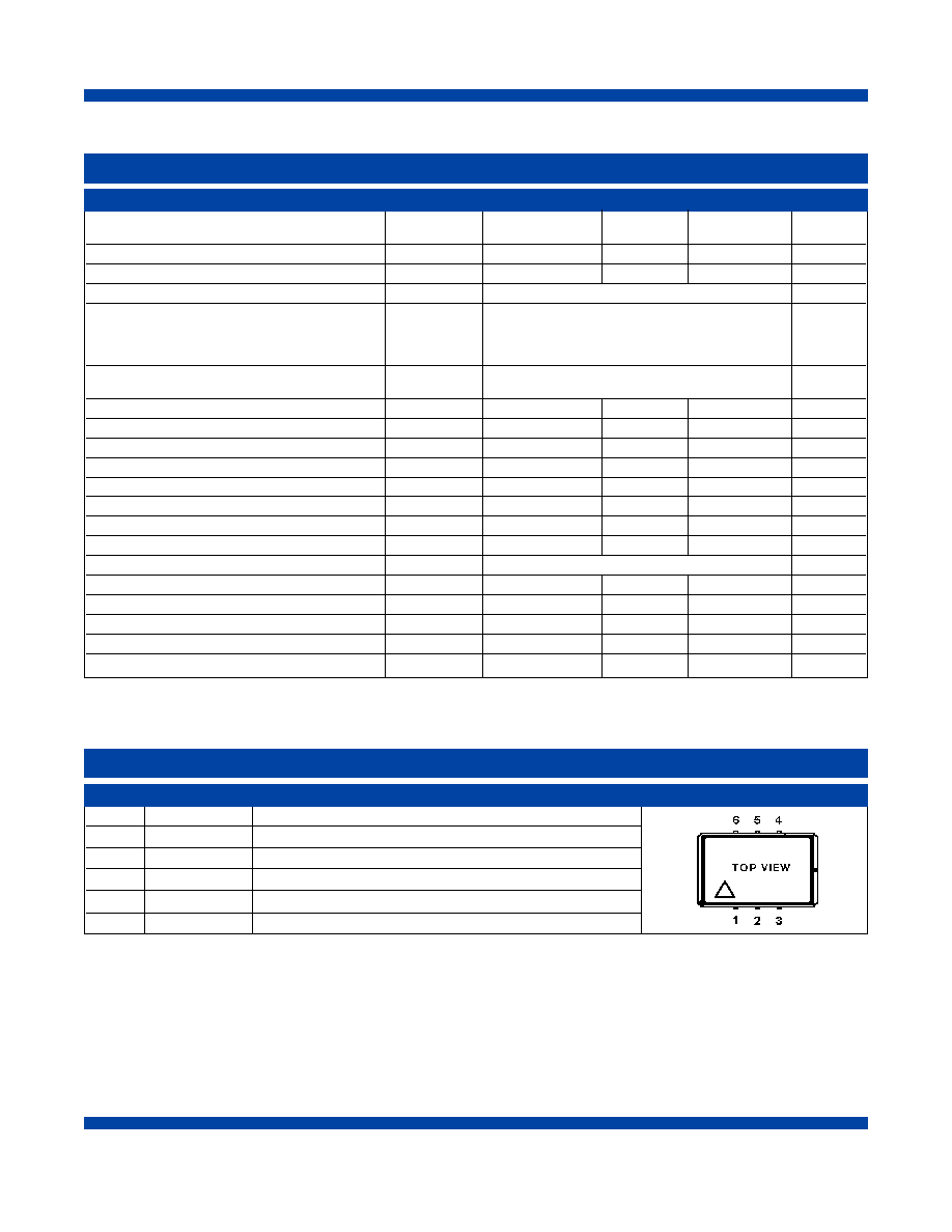
1
Vc VCXO
Control
Voltage.
2
N/C or E/D
1
No Connect or Output Disable option
3
GND
Case and electrical ground.
4
Output
VCXO Output
5
C
Output
VCXO Complementary Output
6
V
CC
Power Supply Voltage (5.0 V or 3.3V ±10%)
Pin Out Information for the PECL output option
Electrical Performance @ 25∞C for the PECL output option
PECL Output Option
1. By setting pin 2 high, the outputs are disabled and output on pin 4 is held low while Complementary output on pin 5 is held high.
Output is enabled by setting pin 2 at < Vcc -1.6V, See ordering information for enable/disable option.
Supply Voltage
1
, +5 volt option
4.5
5.0
5.5
Vdc
+3.3 volt option
3.0
3.3
3.6
Vdc
Supply Current (frequency dependent)
<65mA
Center Frequency, see ordering information
F
N
15
170
MHz
Operating Temperature, see ordering info
T
OP
0/70, -40/85
∞C
Absolute Pull Range over the operating tempera-
APR
±32 to ±50
ppm
ture range, aging and power supply Vc= 0.5 to
4.5 at 5V supply or 0.3 to 3.0 V at 3.3 supply
see ordering information for options
Gain Transfer
K
V
Positive
(Frequency vs. Control Voltage)
Output Level High
2
(0/70∞C)
V
OH
Vcc-1.025
-
Vcc-0.880
V
Output Level Low
2
(0/70∞C)
V
OL
Vcc-1.810
-
Vcc-1.620
V
Output Level High
2
(-40/+85∞C)
V
OH
Vcc-1.085
-
Vcc-0.880
V
Output Level Low
2
(-40/+85∞C)
V
OL
Vcc-1.830
-
Vcc-1.555
V
Output Rise/Fall Time
2
t
R
/ t
F
1
ns
Duty Cycle
SYM
45/55
%
Control Input Leakage
I
L
0.1
mA
Control Voltage Modulation Bandwidth
BW
10
kHz
RMS Jitter
see ordering information
ps
RMS Jitter, 155.52 MHz, 12 kHz to 20 MHz (option P)
0.5
1.0
ps
Maximum Control Voltage
0
V
DD
Maximum Supply Voltage
7
V
Storage Temperature
T
S
-55
-
125
∞C
Soldering Temp./Time
T
LS
-
-
220/10
∞C/s
Parameter
Symbol
Minimum
Typical Maximum
Unit
1. Power supply bypass is required and a 0.1uF in parallel with a 0.01uF high frequency capacitor is recommended.
2. Transition times are measured from 20% to 80% of a full 10K ECL level swing.
Pin
Symbol
Function
J-Type Voltage Controlled Crystal Oscillator
Vectron International ∑
267 Lowell Road, Hudson, NH 03051 ∑ Tel: 1-88-VECTRON-1 ∑ Fax: 1-888-FAX-VECTRON
5
Output Test Conditions (25±5∞C)
PECL Output Option
Ordering Information for the PECL output option (add frequency)
1
J
6 pin
C
5V±10%
U
VCXO
F
±32
C
0/70
M
PECL
U
None
N
Standard
Ceramic 45/55%
SOJ
D 3.3V±10% L
±10%
G
±50
L
-40/85
E
Enable/
P
6ps rms
linear
Disable
(<1ps rms
VCXO
on pin 2
12 kHz-20 MHz)
jitter
M ±20ppm
R
12ps rms
stability
jitter
VCXO
T
20ps rms
jitter
Package
Supply
VCXO
APR
Operating
Output/Duty
Enable/
Specials
Voltage
Type
(ppm)
Temp.
Cycle
Disable
(∞C)
Min/Max
1. Note: Not all combinations are possible.
Example: JDUGLMEP @77.76 MHz = 3.3 volt, VCXO @77.760, ±50 ppm APR, -40/85∞C, 45/55% Symmetry,
PECL, Enable/Disable on pin 2, 6ps rms jitter
77.760
82.944
155.52
Standard Frequencies, in MHz, for PECL output options
Other frequencies available upon request.
Output Wave Form
Output Test Conditions