20
Vectron International ∑ 267 Lowell Road, Hudson, NH 03051 ∑ Tel: 1-88-VECTRON-1 ∑ Web: www.vectron.com
Voltage Controlled Crystal Oscillators (VCXO's)
VC-400/401/410/411/415 Series (CO-600V Series)
Performance Characteristics
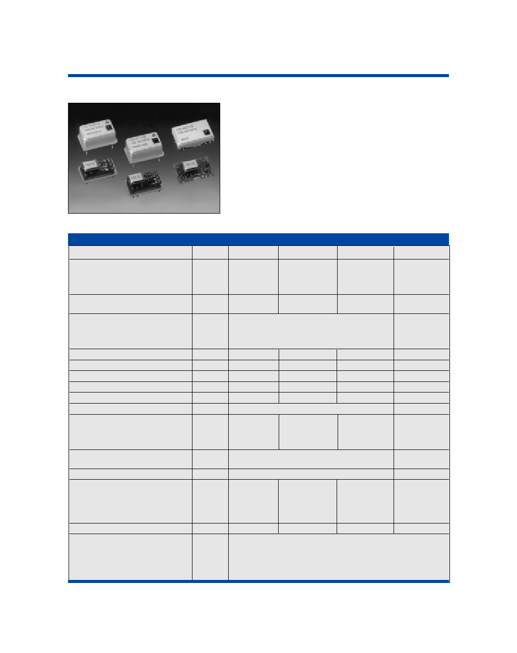
Description:
Low jitter capable, PECL output VCXO in a DIP,
Gull-wing or SMD package.
Features:
∑ 155.52 MHz Standard, Other Frequencies Available from
10 MHz to 170 MHz
∑ Jitter Performance <1 ps rms @ 155.52 MHz
∑ Temperature Stability to ±20 ppm -40∞C to +85∞C
∑ Aging: 10 ppm for 10 Years Typical
∑ ECL or PECL Output
∑ Complementary Output Available
∑ Package: Single DIP, Gull Wing, or True Surface Mount FR4
Standard Frequency:
fo
10
170
MHz
Supply: C
Vdd
4.75
5.0
5.25
V
D
Vdd
3.13
3.3
3.46
V
G
Vdd
-4.94
-5.2
-5.46
V
J
Vdd
-4.27
-4.5
-4.72
V
Current: Single Ended Output
Icc
60
mA
Complementary Output
Icc
50
mA
Output Type: C
ECL
D
PECL
E
Complementary ECL
F
Complementary PECL
Rise/Fall Time (20-80%):
tr/tf
1.5
ns
Symmetry (Duty Cycle):
SYM
45
55
%
Temperature Range:
-40
+85
∞C
Aging (10 years):
10
ppm
Jitter (12 kHz - 20 MHz):
0.5
1
ps
Deviation/Stability:
See How to Order
Control Voltage: PECL, 3.3V
Vc
0.3
3.0
V
PECL, 5V
Vc
0.5
4.5
V
ECL, -4.5V
Vc
-0.5
-4.5
V
ECL, -5.2V
Vc
-0.5
-4.5
V
Transfer Function: PECL
Positive
ECL
Negative
Linearity (BSL):
see ordering information
%
ssb Phase Noise (@ 155.52 MHz)
10Hz
-50
dBc/Hz
(typical)
100Hz
-80
dBc/Hz
1kHz
-115
dBc/Hz
10kHz
-135
dBc/Hz
50kHz
-140
dBc/Hz
Modulation Bandwidth:
BW
10
kHz
Package Size: 400
20.32x12.70x10.8 mm (0.8"x0.5"x0.425") 4 pin DIP
401
20.32x12.70x10.8 mm (0.8"x0.5"x0.425") 5 pin DIP
410
20.32x12.70x11.43 mm (0.8"x0.5"x0.45") 4 pin Gull wing
411
20.32x12.70x11.43 mm (0.8"x0.5"x0.45") 5 pin Gull wing
415
20.32x13.72x5.72 mm (0.8"x0.54"x0.225") SMD
Parameter
Symbol
Minimum
Typical
Maximum
Unit
8798_AA's Vectron 05/30/02 3:11 PM Page 20
Vectron International ∑ 267 Lowell Road, Hudson, NH 03051 ∑ Tel: 1-88-VECTRON-1 ∑ Web: www.vectron.com
21
Voltage Controlled Crystal Oscillators (VCXO's)
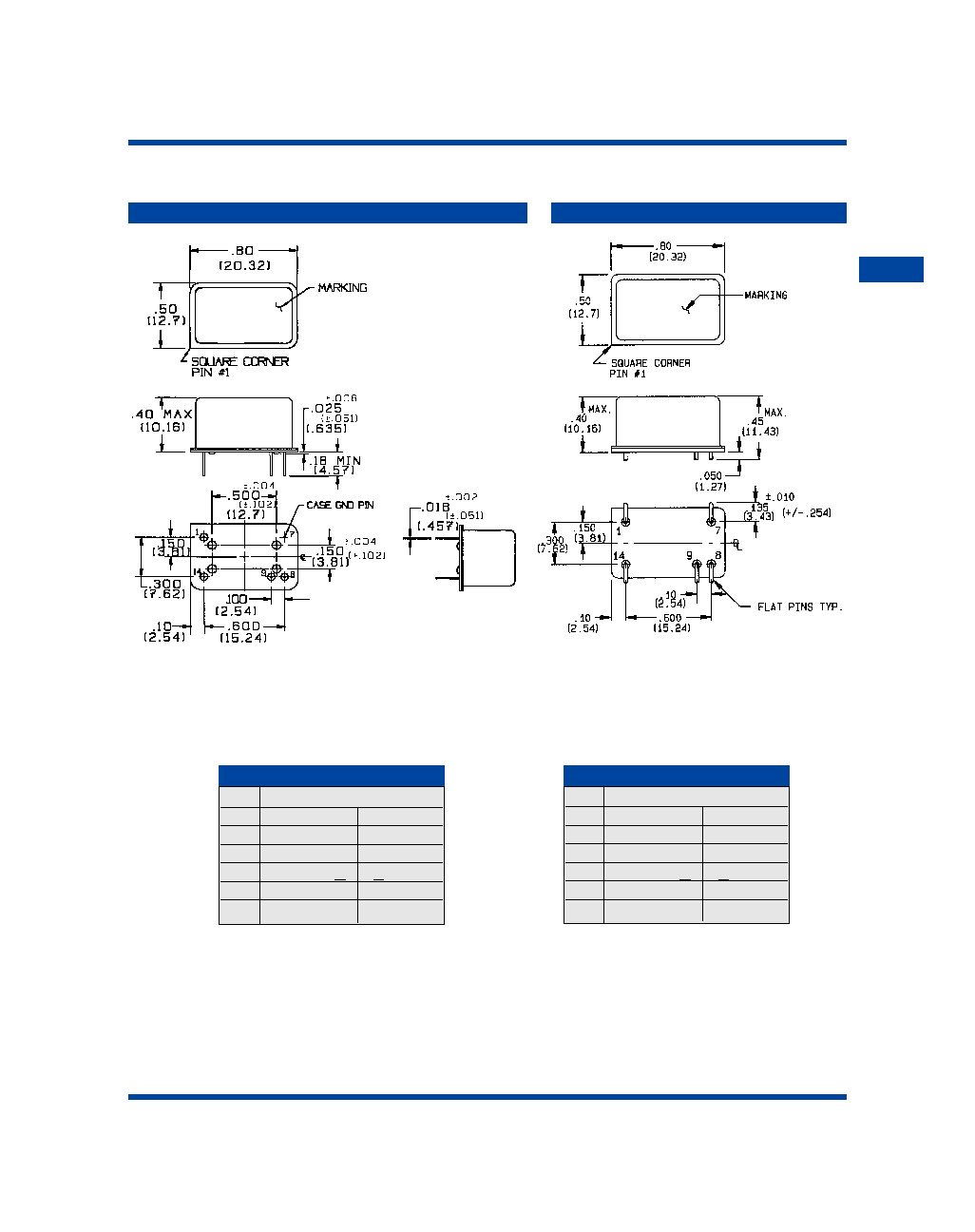
NOTES:
1. Pin numbers are for reference only.
They do not appear on the unit.
2. Dimensions are in inches and (millimeters).
NOTES:
1. Pin numbers are for reference only.
They do not appear on the unit.
2. Dimensions are in inches and (millimeters).
*Pin 9 present only on complementary
output units. Requires 5 pin base.
PIN
FUNCTION
PECL
ECL
1
VCXO
VCXO
7
GROUND
SUPPLY(-)
8
OUTPUT Q
Q
9*
OUTPUT Q
Q
14
SUPPLY(+)
GND
CO-410/411 Outline Drawing
VC-400/401 Outline Drawing
VC-400/401/410/411 Series
Pin Out Information
*Pin 9 present only on complementary
output units. Requires 5 pin base.
PIN
FUNCTION
PECL
ECL
1
VCXO
VCXO
7
GROUND
SUPPLY(-)
8
OUTPUT Q
Q
9*
OUTPUT Q
Q
14
SUPPLY(+)
GND
Pin Out Information
VC-400: 4 pin
VC-401: 5 pin
VC-410: 4 pin
VC-411: 5 pin
V C X O
8798_AA's Vectron 05/30/02 3:11 PM Page 21

22
Vectron International ∑ 267 Lowell Road, Hudson, NH 03051 ∑ Tel: 1-88-VECTRON-1 ∑ Web: www.vectron.com
Voltage Controlled Crystal Oscillators (VCXO's)
NOTES:
1. Pin numbers are for reference only.
They do not appear on the unit.
2. Dimensions are in inches and (millimeters).
*Pin 9 present only on complementary
output units **Disable = PECL high,
oscillator shuts off. Floating or PECL
low normal operation.
PIN
FUNCTION
PECL
ECL
1
VCXO
VCXO
6** DISABLE
DISABLE
7
GNDSUPPLY(-)
8
OUTPUT SIGNAL, Q
Q
9*
OUTPUT SIGNAL, Q
Q
14
SUPPLY(+)
GND
Outline Drawing
Recommended Pad Dimensions
Pin Out Information
VC-415 Series
8798_AA's Vectron 05/30/02 3:11 PM Page 22

Vectron International ∑ 267 Lowell Road, Hudson, NH 03051 ∑ Tel: 1-88-VECTRON-1 ∑ Web: www.vectron.com
23
Voltage Controlled Crystal Oscillators (VCXO's)
Recommended Soldering Profile
Ordering Information
VC
Temperature
Temperature
*Minimum
Code
Range
Stability
Deviation
B-205G
0/+50∞C
±20 ppm
±50 ppm
C-205G
0/+70∞C
±20 ppm
±50 ppm
C-405H
0/+70∞C
±40 ppm
±100 ppm
D-305J
-20/+70∞C
±30 ppm
±60 ppm
D-405H
-20/+70∞C
±40 ppm
±100 ppm
F-405J
-40/+85∞C
±40 ppm
±60 ppm
F-505H
-40/+85∞C
±50 ppm
±100 ppm
F-205G -40/+85∞C
±20 ppm
±50 ppm
Frequency
10 - 170 MHz
400
D
C
205G
155.52
Product Family
VC = VCXO
Supply Voltage
C = 5.0V ±5%
D = 3.3V ±5%
G = -5.2V ±5%
J = -4.5V ±5%
MHz
Package
400 = 4 pin DIP
401 = 5 pin DIP
410 = 4 pin Gullwing
411 = 5 pin Gullwing
415 = SMD
Output
C = ECL
D = PECL
E = Complementary ECL
F = Complementary PECL
VC-400/401/410/411/415 Series
B
V C X O
8798_AA's Vectron 05/30/02 3:11 PM Page 23