 | –≠–ª–µ–∫—Ç—Ä–æ–Ω–Ω—ã–π –∫–æ–º–ø–æ–Ω–µ–Ω—Ç: VC-715 | –°–∫–∞—á–∞—Ç—å:  PDF PDF  ZIP ZIP |

Vectron International, 267 Lowell Rd, Hudson NH 03051-4916
Tel: 1-88-VECTRON-1 Website: www.vectron.com
Page 1 of 5
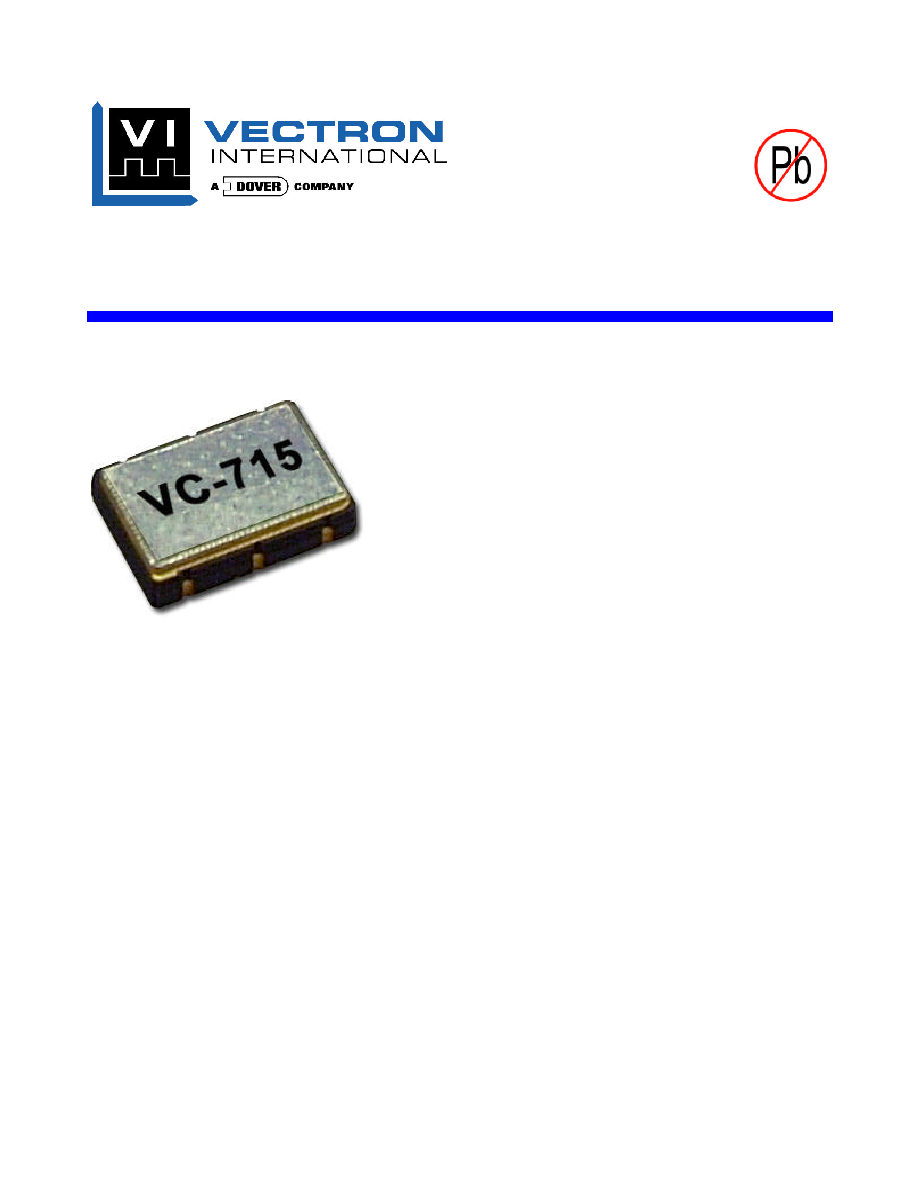
VC-715
LVPECL Voltage Controlled Crystal Oscillator
Features
∑
Small Industry Standard Package, 5.0 x 7.5 x 2.0 mm
∑
19.44 MHz to 77.76 MHz Output Frequency
∑
3.3 V Operation
∑
Fundamental crystal for ultra low jitter
∑
Complementary PECL Outputs
∑
Low phase noise and custom options
∑
0/70 or ≠40/85
∞
C operating temperature
∑
Enable /Disable (PECL)
∑
Lead Free
Applications
PLL circuits for Clock Smoothing and Frequency Translation
∑
Fiber Channel
∑
SONET
∑
SDH, ITU-T G.709
∑
SONET, GR-253-CORE Issue3
Description
The VC-715 is a voltage controlled crystal oscillator that
operates at the fundamental frequency of the internal crystal.
The crystal is a high-Q quartz device that enables the circuit
to achieve low phase jitter performance over a wide
operating temperature range. The oscillator is housed in an
industry standard hermetically sealed leadless surface
mount package and is available on tape and reel.

VC-715 Voltage Controlled Crystal Oscillator
Vectron International, 267 Lowell Rd, Hudson NH 03051-4916
Tel: 1-88-VECTRON-1 Website: www.vectron.com
Page 2 of 6
Electrical Performance
Parameter
Symbol
Min
Typical
Maximum
Units
Frequency
f
O
19.440
77.76
MHz
Supply Voltage (+3.3 V)
V
DD
3.135
3.30
3.465
V
Supply Current
I
DD
<65
mA
Output Logic Levels
Output Logic High 0 / 70 ∫C
Output Logic Low 0 / 70 ∫C
Output Logic High -40 / 85 ∫C
Output Logic Low -40 / 85 ∫C
V
OH
V
OL
V
OH
V
OL
V
DD
-1.025
V
DD
-1.810
V
DD
-1.085
V
DD
-1.830
V
DD
-0.880
V
DD
-1.620
V
DD
-0.880
V
DD
-1.555
V
V
V
V
Transition Times
Rise Time
Fall Time
t
R
t
F
1
1
ns
ns
Symmetry or Duty Cycle
SYM
45
50
55
%
Operating temperature
0/70 or ≠40/85
∞
C
Test Conditions for APR
V
C
0.3
3.0
V
Absolute Pull Range
APR
± 50
ppm
Gain Transfer
Positive
ppm/V
Control Voltage Bandwidth (-3dB)
BW
10
kHz
Input Leakage, Control Voltage Input
±1
uA
Package Size
5.0 x 7.5 x 2.0
mm
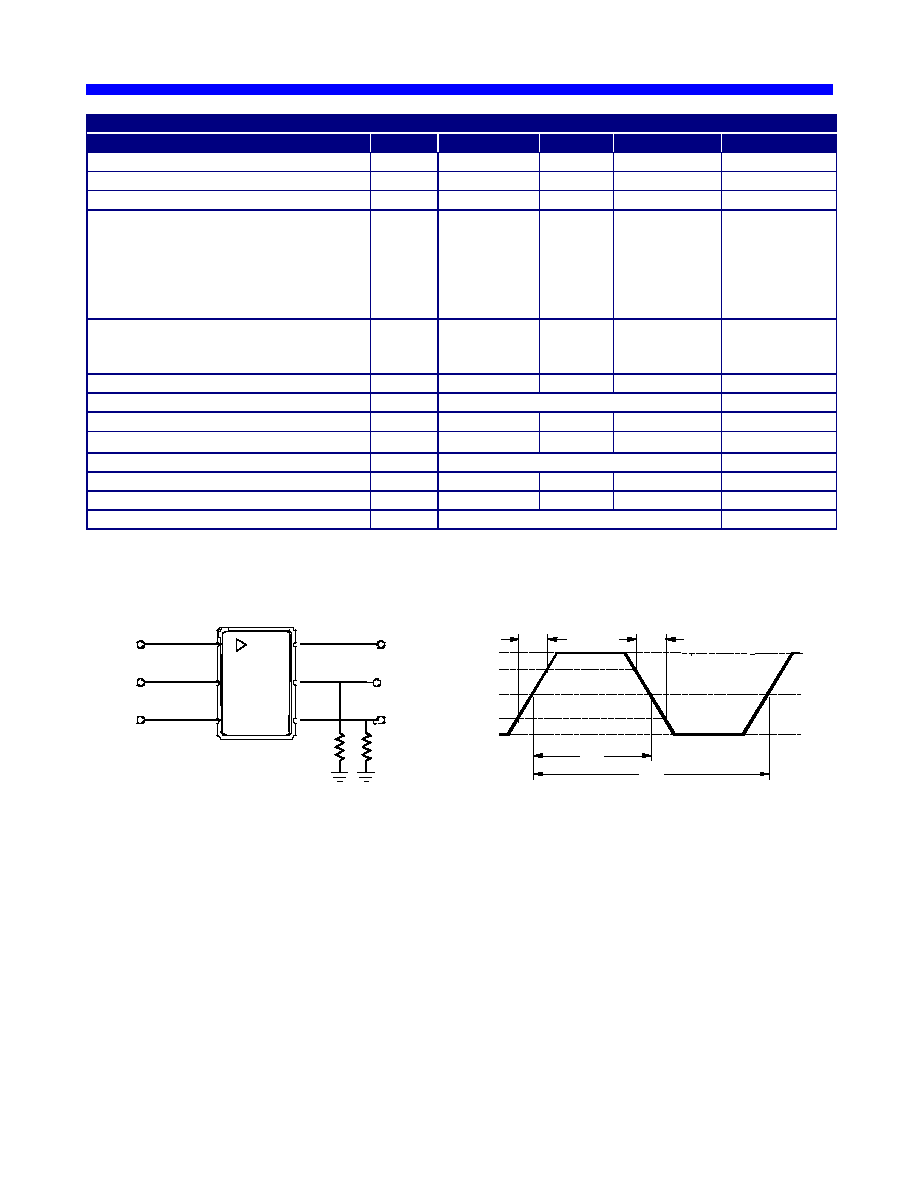
Figure 1 Production Test Circuit
Figure 1. Test Circuit ( 3.3 v)
1
2
3
6
5
4
50
50
Test Circuit Notes:
1) To Permit 50
Measurement of Outputs, all DC Inputs are Biased Down 1.3V.
2) All Voltage Sources Contain Bypass Capacitors to Minimize Supply Noise.
3) 50
Terminations are Within Test Equipment.
(-1.3V to +2V)
( > 0.975V, Open)
(-1.3V)
(+2V)
COutput
Output
Disable, Enable
V
OL
50%
V
OH
80%
20%
t
R
t
F
t
A
t
B
SYM = 100 x t
A
/ t
B
Figure 2. PECL Waveform

VC-715 Voltage Controlled Crystal Oscillator
Vectron International, 267 Lowell Rd, Hudson NH 03051-4916
Tel: 1-88-VECTRON-1 Website: www.vectron.com
Page 3 of 6
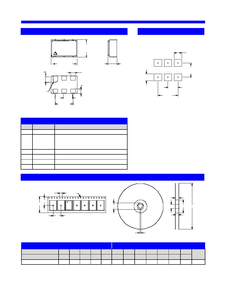
Outline Diagram
Pad Layout
Pin Out
Pin
Symbol
Function
1
V
C
VCXO Control Voltage
2
OE
Output Enable/Disable
Enabled = PECL Logic 1 (or Open)
Disabled = PECL Logic 0
3
GND
Case and Electrical Ground
4
Output
Output
5
COutput
Complementary Output
6
V
CC
Power Supply Voltage (3.3 V)
Tape and Reel (EIA-481-2-A)
Tape Dimensions (mm)
Reel Dimensions (mm)
Dimension
W
F
Do
Po
P1
A
B
C
D
N
W1
W2 # Per
Tolerance
Typ
Typ
Typ
Typ
Typ
Typ
Min
Typ
Min
Min
Typ
Max
Reel
VC-715
16
7.5
1.5
4
8
178
1.5
13
20.2
50
16.4
22.4
200
Po
W
A
N
F
P1
W1
W2
C
B
D
ÿDo
mm
[inch]
5.08
[0.200]
2.54
[0.100]
1.78
[0.070]
3.66
[0.144]
1.96
[0.077]
V C - 7 1 5
X X . X X X
V I Y W W
5 . 0 8 ± 0 . 1 5
[ 0 . 2 0 0 ± 0 . 0 0 6 ]
1 . 4 0
[ 0 . 0 5 5 ]
5 . 0 8
[ 0 . 2 0 0 ]
m m
[ i n c h ]
6
5
4
1
2
3
1 . 2 7
[ 0 . 0 5 0 ]
1 . 9 1
[ 0 . 0 7 5 ]
R 0 . 7 0
[ 0 . 0 2 8 ]
7 . 4 9 ± 0 . 1 5
[ 0 . 2 9 5 ± 0 . 0 0 6 ]
1 . 9 5 ± 0 . 1 8
[ 0 . 0 7 7 ± 0 . 0 0 7 ]
2 . 5 4
[ 0 . 1 0 0 ]

VC-715 Voltage Controlled Crystal Oscillator
Vectron International, 267 Lowell Rd, Hudson NH 03051-4916
Tel: 1-88-VECTRON-1 Website: www.vectron.com
Page 4 of 6
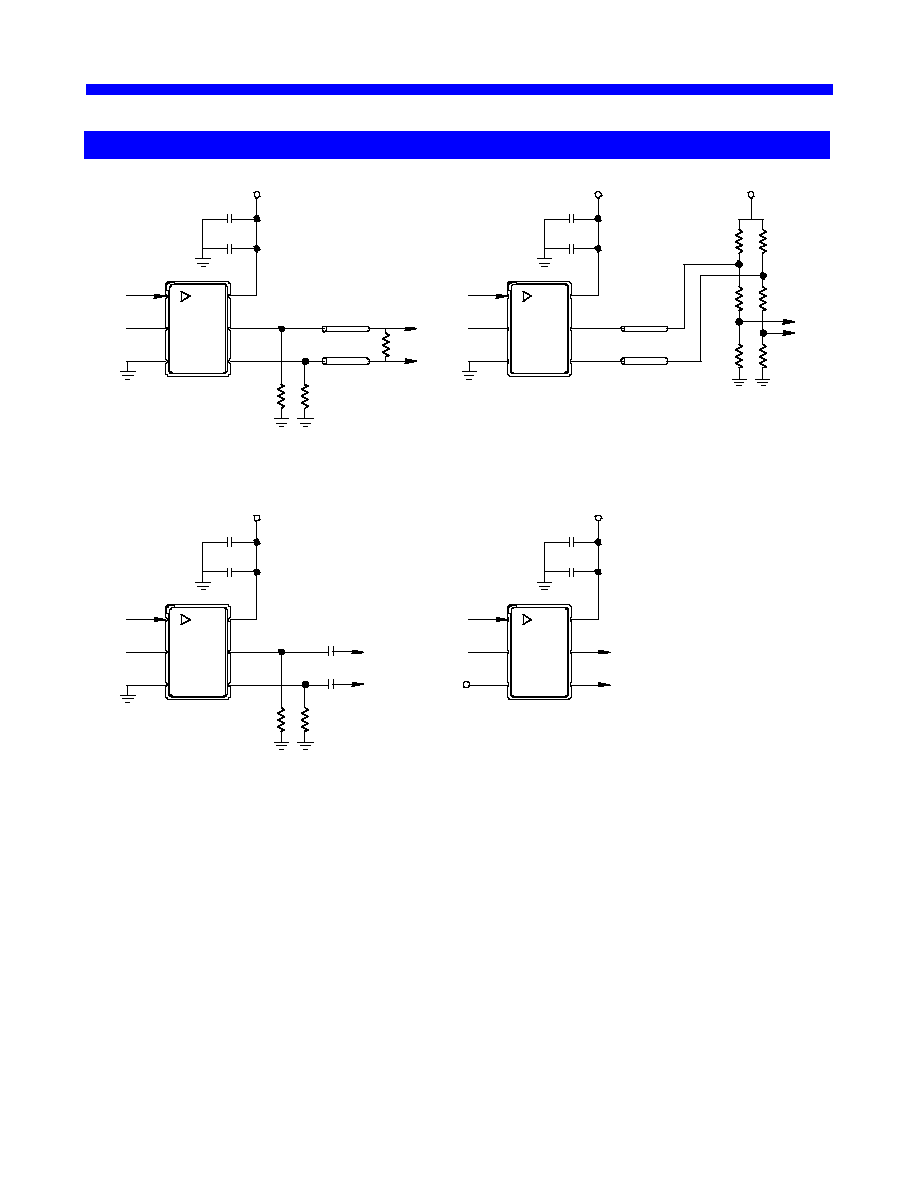
Suggested Output Load Configurations
4
3
240
0.01
µ
F
1
6
2
Gnd
OD
5
Vc
0.10
µ
F
+3.3V
240
100
Z = 50
Z = 50
COutput
Vcc
Output
Gnd
Vc
OD
Output
240
3
4
240
COutput
2
1
5
6
Vcc
0.01
µ
F
0.10
µ
F
+3.3V
OD
-1.3V
COutput
Output
4
3
2
5
Vc
0.01
µ
F
1
6
Vcc
0.10
µ
F
+2.0V
LV-PECL to LV-PECL: For short transmission lengths, the power
consumption could be reduced by removing the 100
resistor and
doubling the value of the pull down resistors.
Functional Test: Allows standard power supply configuration.
Since AC coupled, the LV-PECL levels cannot be measured.
LV-PECL to LVDS: Restricted for short transmission lengths.
Configuration may require modification depending on LVDS receiver.
Gnd
3
Output
4
Z = 50
+3.3V
COutput
OD
Vc
2
1
5
Vcc
6
0.01
µ
F
0.10
µ
F
Z = 50
40
40
150
150
49
49
+3.3V
Production Test: Allows direct DC coupling into 50
measurement
equipment. Must bias the power supplys as shown. Similar to Figure 1.
0.01
µ
F
0.01
µ
F

VC-715 Voltage Controlled Crystal Oscillator
Vectron International, 267 Lowell Rd, Hudson NH 03051-4916
Tel: 1-88-VECTRON-1 Website: www.vectron.com
Page 5 of 6
Absolute Maximum Ratings
Parameter
Symbol
Ratings
Unit
Power Supply
V
CC
0 to 6
V
Output Current
Iout
25
mA
Voltage Control Range
V
C
0 to V
CC
V
Storage Temperature
TS
-55 to 125
∞
C
Soldering Temp/Time
2
T
LS
240/10
∞
C/sec
1) Stresses in excess of the absolute maximum ratings can permanently damage the device. Functional operation is not implied at these
or any other conditions in excess of conditions represented in the operational sections of this data sheet. Exposure to absolute maximum
ratings for extended periods may adversely affect device reliability.
2) Contact pads are gold over nickel, the maximum solder temp can be lower, e.g. 220C.
Reliability
The VC-715 family is capable of meeting the following qualification tests:
Environmental Compliance
Parameter
Conditions
Mechanical Shock
MIL-STD-883, Method 2002
Mechanical Vibration
MIL-STD-883, Method 2007
Solderability
MIL-STD-883, Method 2003
Gross and Fine Leak
MIL-STD-883, Method 1014
Resistance to Solvents
MIL-STD-883, Method 2015
Handling Precautions
Although ESD protection circuitry has been designed into the VC-715 proper precautions should be taken when handling and mounting.
VI employs a human body model and a charged-device model (CDM) for ESD susceptibility testing and design protection evaluation.
ESD Ratings
Model
Minimum
Conditions
Human Body Model
500
MIL-STD 883, Method 3015
Charged Device Model
500
JESD 22-C101
VI qualification includes aging at various extreme temperatures, shock and vibration, temperature cycling, and IR
reflow simulation. The VC-715's are hermetically sealed so an aqueous wash is not an issue. Contact pads are
gold over nickel.
