Vectron International 267 Lowell Road, Hudson NH 03051 Tel: 1-88-VECTRON-1 e-mail: vectron@vectron.com
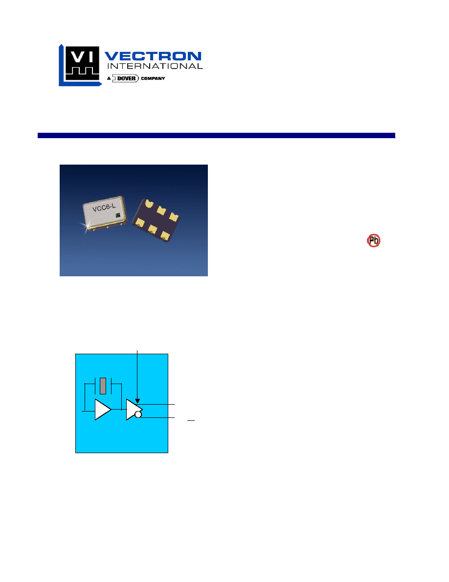
VCC6-L
3.3 volt LVDS Oscillator, >270MHz
The VCC6 Crystal Oscillator
Features
�
3.3 V LVDS
�
Output frequencies from 270-800 MHz
�
Enable/Disable output for test and board debug
�
-10/70 or �40/85
�
C operating temperature
�
Hermetically sealed ceramic SMD package
�
Product is compliant to RoHS directive
and fully compatible with lead free assembly
Applications
�
SONET/SDH/DWDM
�
Ethernet, Gigabit Ethernet
�
Storage Area Network
�
Digital Video
�
Broadband Access
Description
Vectron's VCC6 Crystal Oscillator (XO) is quartz
stabilized square wave generator with a LVDS
output, operating off a 3.3 volt supply.
f
o
f
o
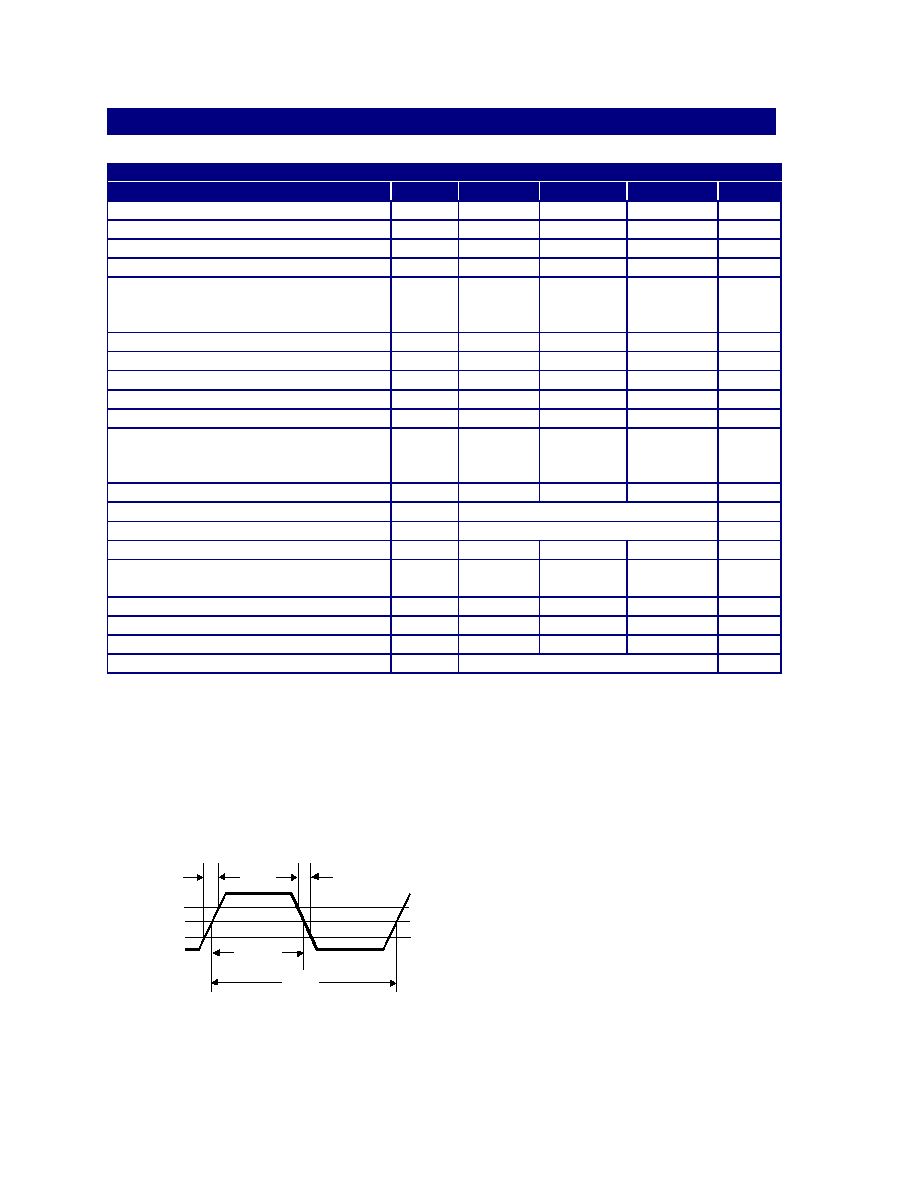
Output
Buffer /
Disable
VCC6-L Output Frequencies > 270MHz
Vectron International 267 Lowell Rd, Hudson NH 03051 Tel: 1-88-VECTRON-1 e-mail: vectron@vectron.com
Performance Characteristics
Table 1. Electrical Performance
Parameter
Symbol
Min
Typical
Maximum
Units
Frequency
f
O
270
800
MHz
Supply Voltage
1
V
DD
3.15
3.3
3.45
Supply Current, Output Enabled
I
DD
80
mA
Supply Current, Output Disabled
I
DD
10
uA
Output Logic Levels
Output Logic High
2
Output Logic Low
2
V
OH
V
OL
0.9
1.40
1.10
1.6
V
V
Differential Output
V
OD
247
330
454
mV
Differential Output Error
50
mV
Offset Voltage
V
OS
1.125
1.25
1.375
V
Offset Error
V
OS
25
mV
Output Leakage Current
�10
uA
Transition Times
Rise Time
2
Fall Time
2
t
R
t
F
600
600
ps
ps
Symmetry or Duty Cycle
3
SYM
45
50
55
%
Operating temperature (ordering option)
-10/70 or �40/85
�
C
Stability (ordering option)
4
�25, �50 or �100
ppm
RMS Jitter, 12kHz to 20 MHz
2
ps
Period RMS Jitter
Period P/P Jitter
4
30
ps
ps
Output Enabled
5
0.7*VDD
V
Output Disabled
5
0.3*VDD
V
Output Enable/Disable time
400
nS
Package Size
5.0 x 7.0 x 1.5
mm
1. A 0.01uF and a 0.1uF capacitor should be located as close to the supply as possible (to ground) is recommended.
2. Figure 1 defines these parameters.
3. Symmetry is measured defined as On Time/Period.
4. Includes calibration tolerance, operating temperature, supply voltage variations, aging (40 degreesC/10 years) and shock and
vibration (not under operation).
5. Output will be enabled if enable/disable is left open.
Figure 1. Output Waveform
80
%
Vs
20
%
t
F
t
R
Period
On Time

VCC6-L Output Frequencies > 270MHz
Vectron International 267 Lowell Rd, Hudson NH 03051 Tel: 1-88-VECTRON-1 e-mail: vectron@vectron.com
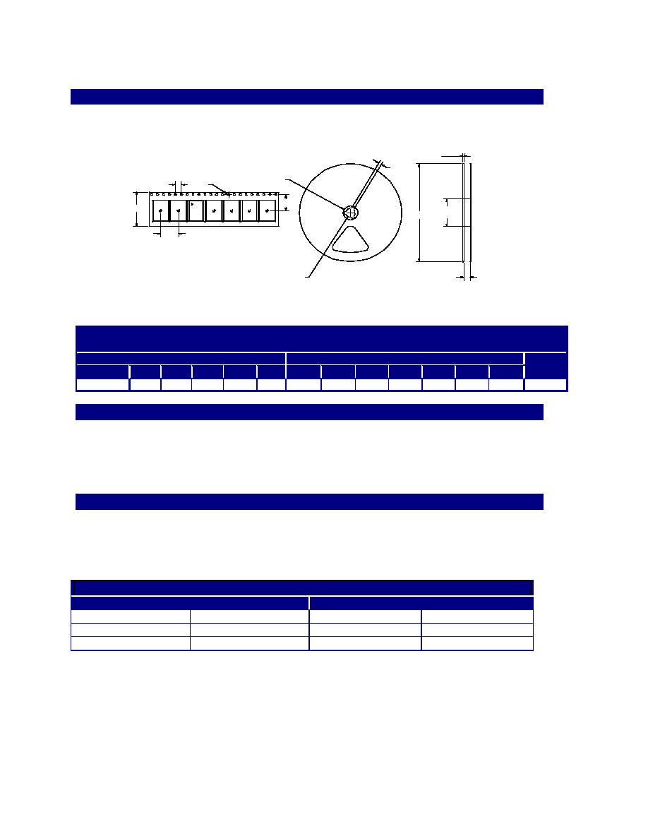
Outline Diagram, Pad Layout and Pin Out
Contact Pad Plating: gold over nickel
Table 2. VCC6-LCx Pinout
Pin #
Symbol
Function
1
E/D
Tristate Function
2
NC
This pin has no internal connection and is floating.
3
GND
Ground
4
f
O
Output Frequency
5
Cf
o
Complementary Output Frequency
6
V
DD
Supply Voltage
Table 3. VCC6-LAx Pinout
Pin #
Symbol
Function
1
NC
This pin has no internal connection and is floating.
2
ED
Tristate Function
3
GND
Ground
4
f
O
Output Frequency
5
Cf
o
Complementary Output Frequency
6
V
DD
Supply Voltage
VCC6-L Output Frequencies > 270MHz
Vectron International 267 Lowell Rd, Hudson NH 03051 Tel: 1-88-VECTRON-1 e-mail: vectron@vectron.com
A
E
C
D
B
G
F
J
L
I
K
H
Tape and Reel
Table 4.
Tape and Reel Dimensions (mm)
Tape Dimensions
Reel Dimensions
# Per
Product
A
B
C
D
E
F
G
H
I
J
K
L
Reel
VCC6
16
7.5
1.5
4
8
2
21
13
60
2
17
180
250
Enable/Disable Functional Description
Under normal operation the Enable/Disable is left open, or set to a logic high state, the VCC6 is an
oscillation mode and outputs are active. When the E/D is set to a logic low, the oscillator stops and the
both the output and complementary outputs are in a high impedance state. This helps facilitate board
testing and troubleshooting.
Absolute Ratings
Stresses in excess of the absolute maximum ratings can permanently damage the device. Functional
operation is not implied at these or any other conditions in excess of conditions represented in the
operational sections of this data sheet. Exposure to absolute maximum ratings for extended periods may
adversely affect device reliability.
Table 5. Absolute Maximum Ratings
Parameter
Symbol
Ratings
Unit
Power Supply
V
DD
-0.5 to +4.6
Vdc
Enable/Disable
V
IN
-0.5 to V
DD
+0.5
Vdc
Storage Temperature
Tstorage
-55/125
�
C
VCC6-L Output Frequencies > 270MHz
Vectron International 267 Lowell Rd, Hudson NH 03051 Tel: 1-88-VECTRON-1 e-mail: vectron@vectron.com
Reliability
The VCC6 qualification tests include the following:
Table 6. Environnemental Compliance
Parameter
Conditions
Mechanical Shock
MIL-STD-883 Method 2002
Mechanical Vibration
MIL-STD-883 Method 2007
Solderability
MIL-STD-883 Method 2003
Gross and Fine Leak
MIL-STD-883 Method 1014
Resistance to Solvents
MIL-STD-883 Method 2016
Handling Precautions
Although ESD protection circuitry has been designed into the the VCC6, proper precautions should be taken
when handling and mounting. VI employs a Human Body Model and a Charged-Device Model (CDM) for
ESD susceptibility testing and design protection evaluation. ESD thresholds are dependent on the circuit
parameters used to define the model. Although no industry wide standard has been adopted for the CDM, a
standard HBM of resistance = 1.5kohms and capacitance = 100pF is widely used and therefore can be
used for comparison purposes.
Table 7. ESD Ratings
Model
Minimum
Conditions
Human Body Model
1000
MIL-STD-883 Method 3115
Charged Device Model
1000
JESD 22-C101
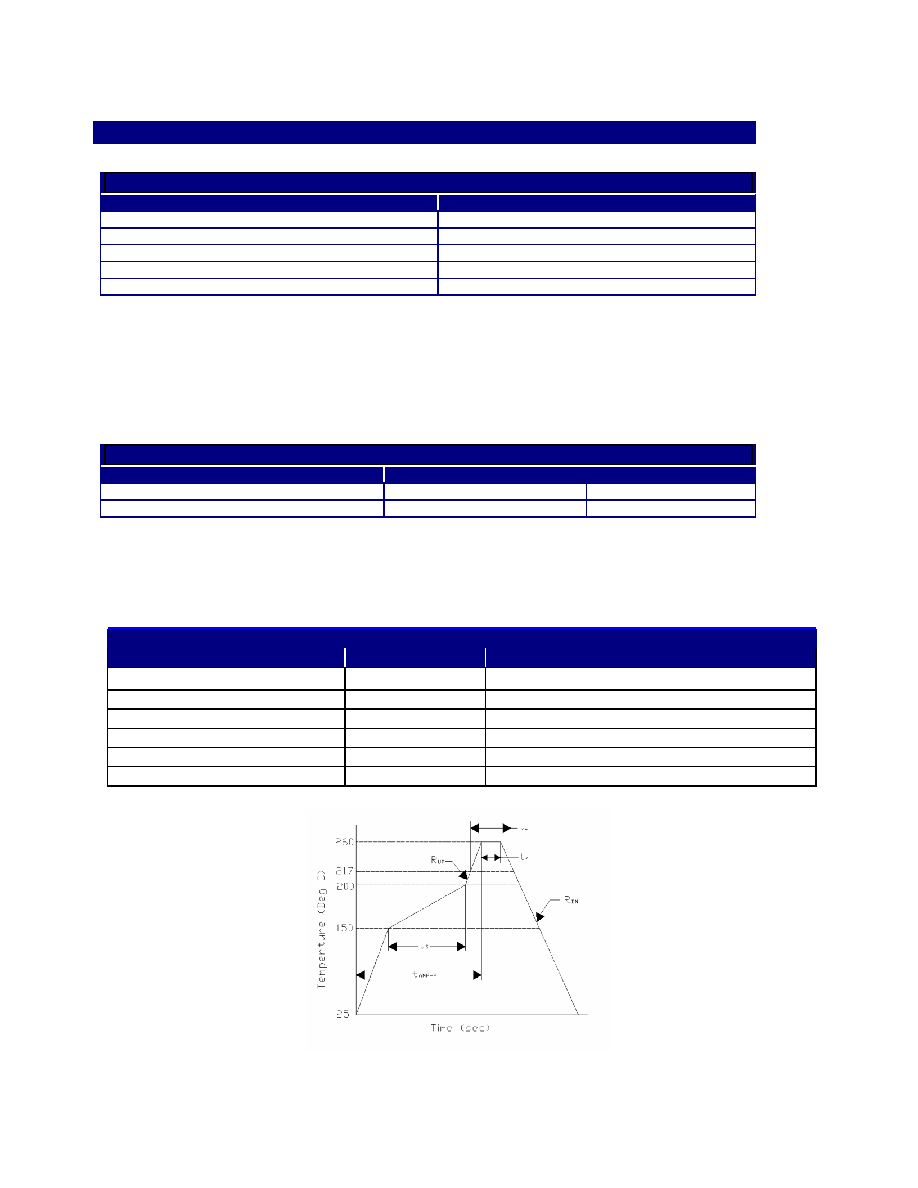
Suggested IR profile
The VCC6 has been qualified to meet the JEDEC standard for Pb-Free assembly. The temperatures and
time intervals listed are based on the Pb-Free small body requirements and parameters are listed in Table 7.
The VCC6 is hermetically sealed so an aqueous wash is not an issue.
Table 8. Reflow Profile
Parameter
Symbol
Value
PreHeat Time
t
S
60 sec Min, 180 sec Max
Ramp Up
R
UP
3
o
C/sec Max
Time Above 217
o
C
t
L
60 sec Min, 150 sec Max
Time To Peak Temperature
t
AMB-P
480 sec Max
Time At 260
o
C (max)
t
P
10 sec Max
Ramp Down
R
DN
6
o
C/sec Max