Vectron International 267 Lowell Road, Hudson NH 03051 Tel: 1-88-VECTRON-1 e-mail: vectron@vectron.com
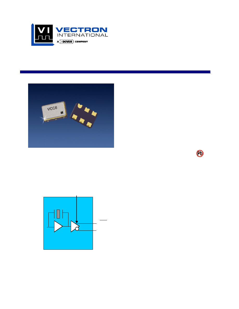
VCC6-Q/R Series
2.5 and 3.3 volt LVPECL Crystal Oscillator
The VCC6 Crystal Oscillator
Features
∑
2.5 or 3.3V LVPECL
∑
3
rd
Overtone Crystal for best jitter performance
∑
Output frequencies to 270 MHz
∑
Low Jitter < 1 pS rms, 12kHz to 20MHz
∑
Enable/Disable for test and board debug
∑
-10/70 or ≠40/85
∞
C operating temperature
∑
Hermetically sealed ceramic SMD package
∑
Product is compliant to RoHS directive
Applications
∑
SONET/SDH/DWDM
∑
Fiber Channel
∑
Ethernet, Gigabit Ethernet
∑
Storage Area Network
∑
Digital Video
∑
Broadband Access
Description
Vectron's VCC6 Crystal Oscillator (XO) is quartz
stabilized square wave generator with a LV-PECL
output, operating off a 3.3 volt supply.
The VCC6 uses 3
rd
overtone crystals for
frequencies under 200MHz, resulting in low jitter
performance, typically 0.3pS rms in the 12 kHz to
20MHz band.
OUT
Output
Buffer /
Disable
Enable/Disable
OUT
VCC6-Q/R Series, 2.5 and 3.3v PECL Crystal Oscillator
Vectron International 267 Lowell Rd, Hudson NH 03051 Tel: 1-88-VECTRON-1 e-mail: vectron@vectron.com
Performance Characteristics
Table 1. Electrical Performance
Parameter
Symbol
Min
Typical
Maximum
Units
Frequency
f
O
10
270
MHz
Supply Voltage
1
, 3.3V Q option
2.5V R option
V
DD
3.15
2.375
3.3
2.5
3.45
2.625
V
Supply Current
I
DD
98
mA
Output Logic Levels, 0/70∞C
Output Logic High
2
Output Logic Low
2
V
OH
V
OL
V
DD
-1.025
V
DD
-1.810
V
DD
-0.880
V
DD
-1.620
V
V
Output Logic Levels, -40/85∞C
Output Logic High
2
Output Logic Low
2
V
OH
V
OL
V
DD
-1.085
V
DD
-1.830
V
DD
-0.880
V
DD
-1.555
V
V
Transition Times
Rise Time
2
Fall Time
2
t
R
t
F
600
600
ps
ps
Symmetry or Duty Cycle
3
SYM
45
50
55
%
Operating temperature (ordering option)
T
OP
-10/70 or ≠40/85
∞
C
Stability (ordering option)
4
deltaF/F
±25, ±50 or ±100
ppm
Jitter, 12kHz to 20MHz
5
Cycle to Cycle, rms
Cycle to Cycle, peak-peak
Period Jitter, rms
Period Jitter, peak-peak
0.3
4.8
38
2.7
23
0.7
pS
Output Enabled
6
V
IH
0.7*V
DD
V
Output Disabled
6
V
IL
0.3*V
DD
V
Output Enable/Disable time
t
E/D
200
nS
Enable/Disable Leakage Current
I
IL
±
200
uA
Output Enable Pull-Up Resistor
6
Output Enabled
Output Disabled
33
1
Kohm
Mohm
1. A 0.01uF and a 0.1uF capacitor should be located as close to the supply as possible and terminated to ground.
2. Figure 1 defines these parameters. Figure 2 illustrates the operating conditions under which these parameters are tested and specified.
3. Symmetry is measured defined as On Time/Period.
4. Includes calibration tolerance, operating temperature, supply voltage variations, aging (40 degreesC/10 years) and shock and vibration (not under
operation).
5. Measurements made on a VCC6-QAB-155M520 using an Agilent E5052A for phase noise and LeCroy 8600, 25K samples for jitter.
6. Output will be enabled if Enable/Disable is left open. The pull resistor changes to a higher value, operating in a "power saving mode" when
Enable/Disable is set to a logic 0.
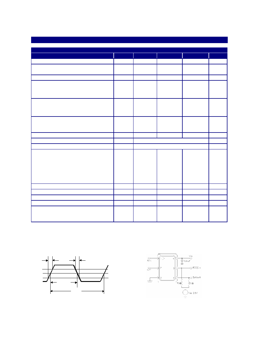
Figure 1. Output Waveform
Figure 2. Typical Output Test Conditions (25
±
5∞C)
80
%
Vs
20
%
t
F
t
R
Period
On Time

VCC6-Q/R Series, 2.5 and 3.3v PECL Crystal Oscillator
Vectron International 267 Lowell Rd, Hudson NH 03051 Tel: 1-88-VECTRON-1 e-mail: vectron@vectron.com
Outline Diagram and Pin Out
Table 2. VCC6-QAx Pinout
Pin #
Symbol
Function
1
NC
This pin has no internal connection and is floating.
2
E/D
Enable/Disable Function
3
GND
Ground
4
f
O
Output Frequency
5
Cf
o
Complementary Output Frequency
6
V
DD
Supply Voltage
Gold over Nickel plating
Figure 3 Optional VCC6-QAx Package Drawing
Table 3. VCC6-QCx Pinout
Pin #
Symbol
Function
1
E/D
Enable/Disable Function
2
NC
This pin has no internal connection and is floating.
3
GND
Ground
4
f
O
Output Frequency
5
Cf
o
Complementary Output Frequency
6
V
DD
Supply Voltage
Gold over Nickel plating
Figure 4. VCC6-QCx and VCC6-QAx Package Drawing
VCC6-Q/R Series, 2.5 and 3.3v PECL Crystal Oscillator
Vectron International 267 Lowell Rd, Hudson NH 03051 Tel: 1-88-VECTRON-1 e-mail: vectron@vectron.com
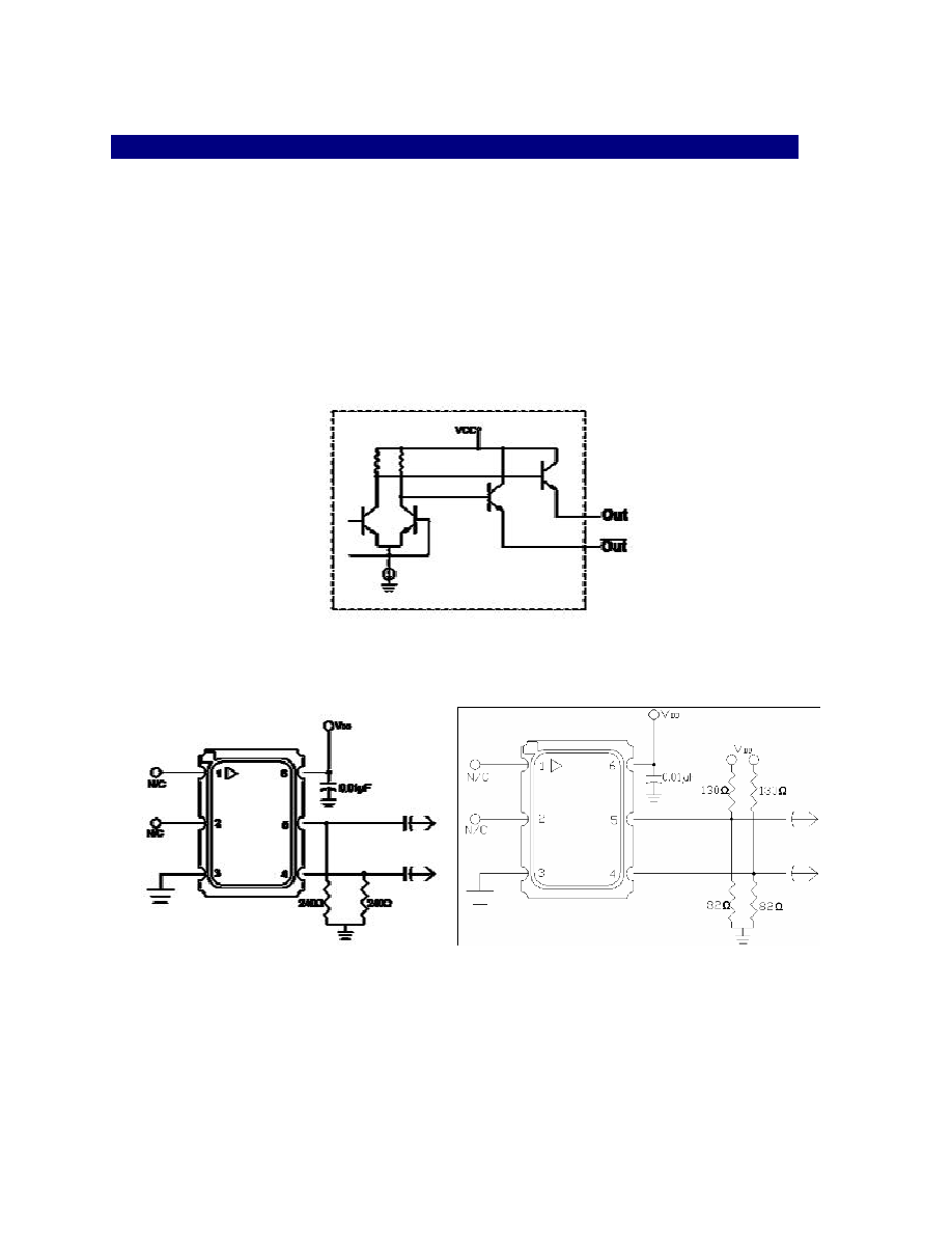
Terminating PECL Outputs
The VCC6 incorporates a standard PECL output scheme, which are un-terminated emitters as shown in
Figure 5. There are numerous application notes on terminating and interfacing PECL logic and the two most
common methods are a single resistor to ground, Figure 6, and a pull-up/pull-down scheme as shown in
Figure 7. An AC coupling capacitor is optional, depending on the application and the input logic
requirements of the next stage.
One of the most important considerations is terminating the Output and Complementary Outputs equally.
An unused output should not be left un-terminated, and if it one of the two outputs is left open it will result in
excessive jitter on both. PC board layout must take this and 50 ohm impedance matching into account.
Load matching and power supply noise are the main contributors to jitter related problems.
Figure 5. Standard PECL Output Configuration
Figure 6. Single Resistor Termination
Figure 7. Pull-up Pull-down Termination
Resistor value are typically:
Resistor values are typically:
120 to 240ohms for 3.3V
130 and 82 ohms for 3.3V
82 to 120 ohms for 2.5V
240 and 62 ohms for 2.5V
VCC6-Q/R Series, 2.5 and 3.3v PECL Crystal Oscillator
Vectron International 267 Lowell Rd, Hudson NH 03051 Tel: 1-88-VECTRON-1 e-mail: vectron@vectron.com
Enable/Disable Functional Description
Under normal operation the Enable/Disable is left open, or set to a logic high state, and the VCC6 is in
oscillation mode and outputs are enabled (active). When the E/D is set to a logic low, the oscillator stops
and the both the output and complementary outputs are in a high impedance state. This helps facilitate
board testing and troubleshooting.
Power Saving Pull-Up Resistor
The E/D pull-up resistor changes in response to the input logic level; the pull-up resistor is a large value
when E/D is set to a logic low, which reduces the current consumed. When E/D is open, or set to a logic
high, the pull-up resistance becomes a smaller value which helps decrease the effects of external noise.
Absolute Maximum Ratings
Stresses in excess of the absolute maximum ratings can permanently damage the device. Functional
operation is not implied at these or any other conditions in excess of conditions represented in the
operational sections of this data sheet. Exposure to absolute maximum ratings for extended periods may
adversely affect device reliability.
Table 4. Absolute Maximum Ratings
Parameter
Symbol
Ratings
Unit
Power Supply
V
DD
-0.5 to +7.0
Vdc
Enable/Disable
V
IN
-0.5 to V
DD
+0.5
Vdc
Storage Temperature
Tstorage
-55/125
∞
C
Reliability
The VCC6 qualification tests included:
Table 5. Environnemental Compliance
Parameter
Conditions
Mechanical Shock
MIL-STD-883 Method 2002
Mechanical Vibration
MIL-STD-883 Method 2007
Solderability
MIL-STD-883 Method 2003
Gross and Fine Leak
MIL-STD-883 Method 1014
Resistance to Solvents
MIL-STD-883 Method 2016
Handling Precautions
Although ESD protection circuitry has been designed into the the VCC6, proper precautions should be taken
when handling and mounting. VI employs a Human Body Model and a Charged-Device Model (CDM) for
ESD susceptibility testing and design protection evaluation. ESD thresholds are dependent on the circuit
parameters used to define the model. Although no industry wide standard has been adopted for the CDM, a
standard HBM of resistance = 1.5kohms and capacitance = 100pF is widely used and therefore can be
used for comparison purposes.
Table 6. ESD Ratings
Model
Minimum
Conditions
Human Body Model
1500
MIL-STD-883 Method 3015
Charged Device Model
1000