Äîêóìåíòàöèÿ è îïèñàíèÿ www.docs.chipfind.ru
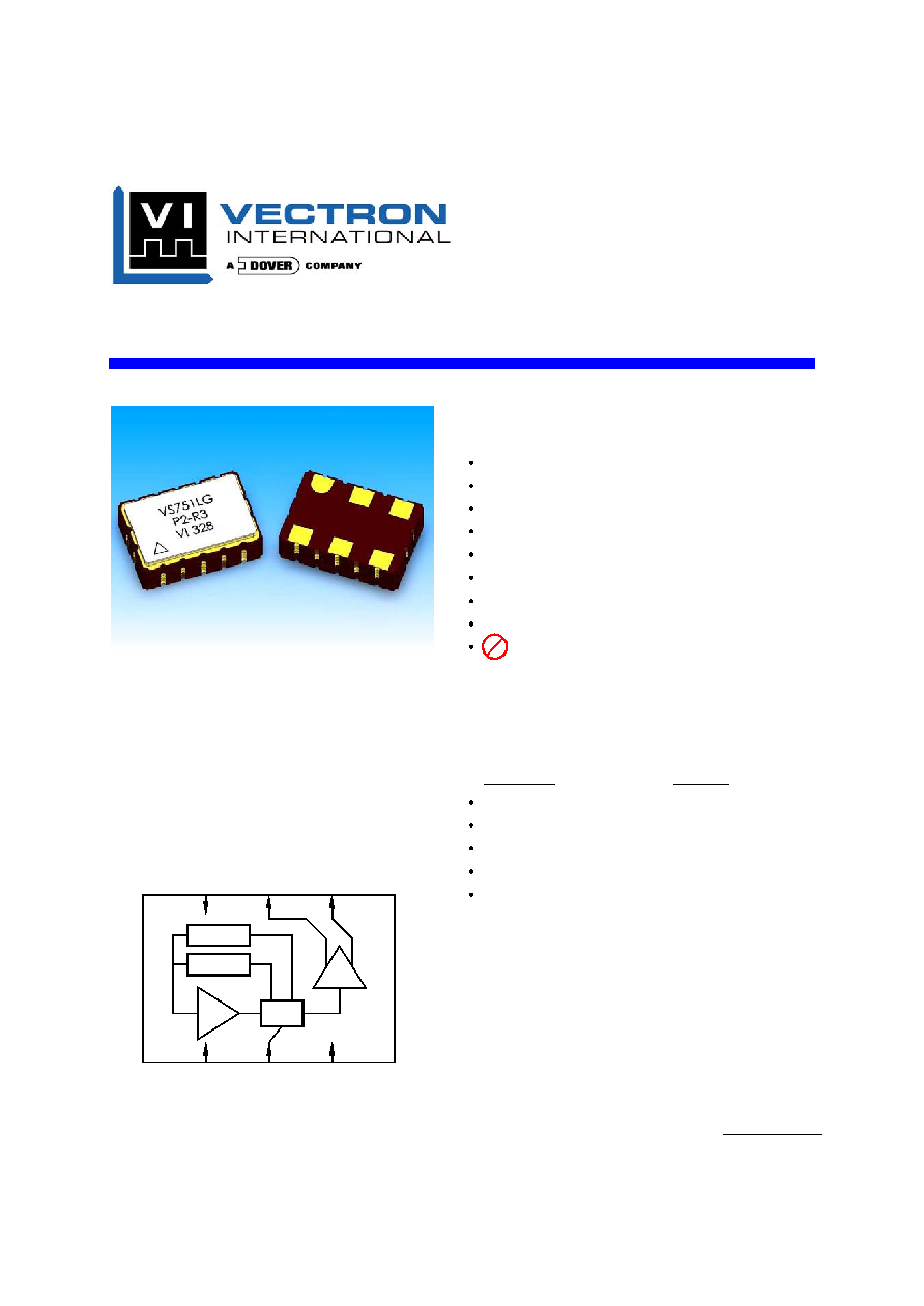
VS-751
Dual Frequency VCSO
Vectron International, 267 Lowell Rd, Hudson NH 03051-4916
Tel: 1-88-VECTRON-1
Website: www.vectron.com
Page 1 of 7
Rev: 09Jan06
Features
5 x 7.5 x 2.5 mm Package
Output Frequencies from 500 MHz to 850 MHz
3.3 V Operation
Low Jitter < 0.25 ps-rms across 50 kHz to 80 MHz
LV-PECL Configuration with Fast Transition Times
Complementary Outputs
Frequency Select
Patent Pending Technology
Product is free of lead and compliant to
EC RoHS Directive
Applications
PLL circuits for Clock Smoothing and Frequency Translation
Description
Standard
1-2-4 Gigabit Fibre Channel
INCITS 352-2002
10 Gigabit Fibre Channel
INCITS 364-2003
10GbE LAN / WAN
IEEE 802.3ae
OC-192
ITU-T G.709
SONET / SDH
GR-253-CORE Issue3
Description
The VS-751 is a SAW based voltage controlled oscillator that
operates at the fundamental frequencies of the internal SAW
filters. These SAW filters are high-Q quartz devices that
enable the circuit to achieve low phase jitter performance over
a wide operating temperature range. The dual oscillator is
housed in a hermetically sealed leadless surface mount
package offered on tape and reel. It has a frequency select
function that enables either
"
Frequency 1
"
or
"
Frequency 2.
"
Pb
FS
Vc
Gnd
Output
COutput
Vcc
SAW 1
SAW 2
VS-751 Voltage Controlled SAW Oscillator
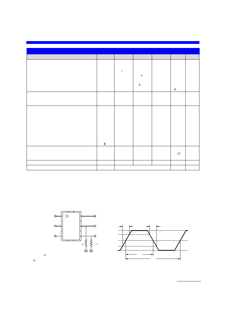
Electrical Performance
Parameter
Symbol
Minimum
Typical
Maximum
Units
Notes
Frequency
Nominal Frequency
Absolute Pull Range
Linearity
Gain Transfer (See Pg 5)
Temperature Stability
Transition Time
f
N
APR
Lin
K
V
f
STAB
50
500 - 850
5
+405
100
4
MHz
ppm
%
ppm/V
ppm
sec
1,2,3
1,2,3,8
2,4,8
2,8
1,6
6
Supply
Voltage
Current (No Load)
V
CC
I
CC
2.97
3.3
55
3.63
70
V
mA
2,3
3
Outputs
Mid Level
Swing
Current
Rise Time
Fall Time
Symmetry
Spurious Suppression
Jitter (See Pg 5)
I
OUT
t
R
t
F
SYM
J
V
CC
-1.4
550
45
50
V
CC
-1.3
650
250
250
50
60
0.130
V
CC
-1.2
950
20
400
400
55
0.250
V
mV-pp
mA
ps
ps
%
dBc
ps-rms
2,3
2,3
6
5,6
5,6
2,3
6
6,7
Control Voltage
Input Impedance
Modulation Bandwidth
Z
C
BW
100
500
k
kHz
6
6
Operating Temperature
T
OP
-40
85
°
C
1,3
Package Size
5.0 x 7.5 x 2.5
mm
1. See Standard Frequencies and Ordering Information (Pg 7).
2. Parameters are tested with production test circuit below (Fig 1).
3. Parameters are tested at ambient temperature with test limits guardbanded for specified operating temperature.
4. Measured as the maximum deviation from the best straight-line fit, per MIL-0-55310.
5. Measured from 20% to 80% of a full output swing (Fig 2).
6. Not tested in production, guaranteed by design, verified at qualification.
7. Integrated across 50 kHz to 80 MHz, per GR-253-CORE Issue3.
8. Tested with Vc = 0.3V to 3.0V.
Figure 1. Test Circuit
Figure 2. 10K LV-PECL Waveform
Vcc - 1.6V
Vcc - 1.3V
Vcc - 1.0V
80%
20%
1
2
3
6
5
4
50
50
t
R
t
F
t
A
t
B
SYM = 100 x t
A
/ t
B
Test Circuit Notes:
To Permit 50 Measurement of Outputs, all DC Inputs are Biased Down 1.3V.
All Voltage Sources Contain Bypass Capacitors to Minimize Supply Noise.
Terminations are Within Test Equipment.
Vc (-1.0V to +1.7V)
Vee (-1.3V)
Vcc (+2V)
COutput
Output
), F2 (+0.59V)
1)
2)
3) 50
F1 (-0.58V
Vectron International, 267 Lowell Rd, Hudson NH 03051-4916
Tel: 1-88-VECTRON-1 Website: www.vectron.com
Page 2 of 7
Rev: 09Jan06
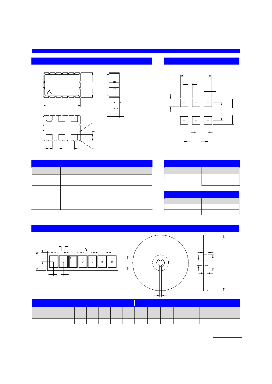
VS-751 Voltage Controlled SAW Oscillator
VS751LG
XX - XX
VI YWW
5.10
±
0.15
[0.201
±
0.006]
mm
[inch]
6
5
4
1
2
3
7.50
±
0.15
[0.295
±
0.006]
2.49
±
0.18
[0.098
±
0.007]
2.54
[0.100]
1.30
[0.051]
Y = Year
WW = Week
XX = Frequency Code
(See Ordering Info)
1.27
[0
mm
[inch]
5.08
[0.200]
2.54
[0.100]
3.83
[0.151]
1.68
[0.066]
1.70
[0.067]
0.86
[0.034]
5.54
[0.218]
6.76
[0.266]
Outline Diagram
Pad Layout
.050]
1.27
[0.050]
4X R0.19
[R0.007]
R0.15
[R0.006]
0.68
[0.027]
Pin Out
Marking Key
Pin
Symbol
Function
Position 6
Position 7
1
V
C
VCSO Control Voltage
L = LFF
G = GNN
2
FS
Frequency Select (See Control Logic)
H = HNN
3
Gnd
Case and Electrical Ground
4
Output
VCSO Output
Control Logic (LV-CMOS)
5
COutput
VCSO Complementary Output
FS
Operation
6
V
CC
Power Supply Voltage (3.3 V 10%)
0
F1
1
F2
Tape and Reel (EIA-481-2-A)
Tape Dimensions (mm)
Reel Dimensions (mm)
Dimension
W
F
Do
Po
P1
A
B
C
D
N
W1
W2
# Per
Tolerance
Typ
Typ
Typ
Typ
Typ
Typ
Min
Typ
Min
Min
Typ
Max
Reel
VS-751
16
7.5
1.5
4
8
178
1.5
13
20.2
50
16.4
22.4
200
Vectron International, 267 Lowell Rd, Hudson NH 03051-4916
Tel: 1-88-VECTRON-1 Website: www.vectron.com
Page 3 of 7
Rev: 09Jan06
Po
W
A
N
F
P1
W1
W2
C
B
D
Ø
Do
VS-751 Voltage Controlled SAW Oscillator
Absolute Maximum Ratings
Parameter
Symbol
Ratings
Unit
Power Supply
V
CC
0 to 6
V
Input Current
I
IN
100
mA
Output Current
I
OUT
25
mA
Voltage Control Range
V
C
0 to V
CC
V
Storage Temperature
T
STR
-55 to 125
C
Soldering Temperature / Duration
T
PEAK
/ t
P
260 / 40
C / sec
Stresses in excess of the absolute maximum ratings can permanently damage the device. Also, exposure to
these absolute maximum ratings for extended periods may adversely affect device reliability. Functional
operation is not implied at these or any other conditions in excess of those represented in the operational
sections of this datasheet. Permanent damage is also possible if any device input (Vc or FS) draws greater
than 100mA.
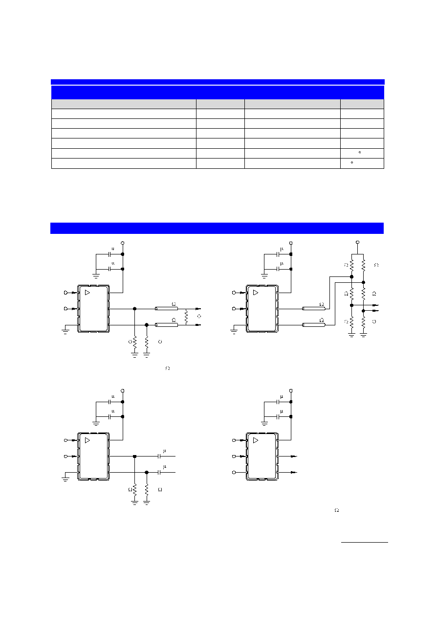
Suggested Output Load Configurations
4
3
240
0.01 F
1
6
2
Gnd
FS
5
Vc
0.10 F
+3.3V
240
100
Z = 50
Z = 50
COutput
Vcc
Output
240
240
LV-PECL to LV-PECL: For short transmission lengths, the power
onsumption could be reduced by removing the 100 resistor and
ubling the value of the pull down resistors.
unctional Test: Allows standard power supply configuration.
ince AC coupled, the LV-PECL levels cannot be measured.
LV-PECL to LVDS: Restricted for short transmission lengths.
Configuration may require modification depending on LVDS receiver.
c
do
F
S
Z = 50
Z = 50
40
40
150
150
49
49
+3.3V
Production Test: Allows direct DC coupling into 50 measurement
equipment. Must bias the power supplys as shown. Similar to Figure 1.
0.01 F
0.01 F
+3.3V
Vc
1
6
Vcc
0.01 F
0.10 F
Gnd
3
4
FS
2
5
COutput
Output
+2.0V
Vc
1
6
Vcc
0.01 F
0.10 F
-1.3V
3
4
FS
2
5
COutput
Output
+3.3V
Vc
1
6
Vcc
0.01 F
0.10 F
Gnd
3
4
FS
2
5
COutput
Output
Vectron International, 267 Lowell Rd, Hudson NH 03051-4916
Tel: 1-88-VECTRON-1 Website: www.vectron.com
Page 4 of 7
Rev: 09Jan06
VS-751 Voltage Controlled SAW Oscillator
Typical Characteristics
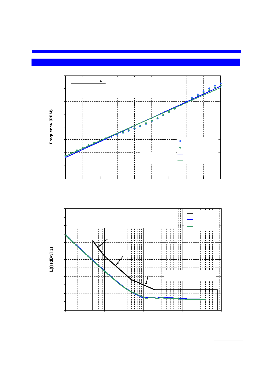
y = 415.29x - 605.56
y = 398.69x - 578.48
-800
-600
-400
-200
0
200
400
600
800
0.3
0.6
0.9
1.2
1.5
1.8
2.1
2.4
2.7
3
Control Voltage (V)
622 Vc Pull
644 Vc Pull
Linear (622 Vc Pull)
Linear (644 Vc Pull)
At Ambient (22.5 C)
Typical Gain Transfer @ 622.0800 = +415 ppm/V
Typical Gain Transfer @ 644.5313 = +399 ppm/V
-155
-150
-145
-140
-135
-130
-125
-120
-115
-110
-105
-100
-95
10
100
1,000
10,000
100,000
Offset (kHz)
OC-192 Spec
F1 = 622
F2 = 644
1/f
3
1/f
2
1/f
1
OC-192 Spec Equivalent to
0.25 ps-rms @ 500 MHz
Typical Calculated Jitter @ Vc = 1.65V
SONET OC-48 (12kHz-20MHz) = 0.23 ps-rms; 1.61 ps-pp
SONET OC-192 (50kHz-80MHz) = 0.13 ps-rms; 0.91 ps-pp
Vectron International, 267 Lowell Rd, Hudson NH 03051-4916
Tel: 1-88-VECTRON-1 Website: www.vectron.com
Page 5 of 7
Rev: 09Jan06