
Vicor Corporation Tel: 800-735-6200 vicorpower.com V∑I Chip Evaluation Board Rev.
1.2 Page 1 - 4
4
5
PRELIMIN
ARY
The V∑I Chip evaluation board offers a convenient means to
evaluate the performance of Vicor's Bus Converter Modules
(BCM) or Voltage Transformation Modules (VTM).
The board has been optimized for user convenience.
Refer to the appropriate V∑I Chip datasheet for performance
and operating limits. The datasheets are available for
downloading at vicorpower.com.
It is important to remember that given the fast response of most
V∑I Chips, they can readily show the limitations of the source,
load, and associated wiring connected to the evaluation board.
Care should be exercised to minimize stray source and load
impedances in order to fully exercise the V∑I Chip.
Please refer to Figure 1 for locations of the input and output
connections as viewed from the component side. Wires may be
soldered directly to the pads in lieu of ring lugs if desired to
minimize circuit impedances.
The evaluation board should be set up as follows:
Note: Care should be taken to avoid reversing polarities
if connecting to the opposite (solder) side of the board.
1. + IN, - IN
Connect a high quality, low noise power supply to this
location. The interconnect leads should be heavy gauge
and as short as possible. Additional capacitance may
have to be added on the evaluation board to make up
for impedances in the interconnect leads as well as
deficiencies in the source. It is important to remember
that noise from the source, as well as any input source
voltage drops, will appear at the output of the V∑I Chip
multiplied by its k factor.
2. + OUT, -OUT
An electronic or passive load should be connected to this
location with short heavy gauge leads. Most commercially
available electronic loads do not have current slew rates
capable of exercising the V∑I Chips capability. The evaluation
board can be connected directly to the application for which
the V∑I Chip is intended; however, the interconnect
impedances between the evaluation board and the application
can greatly effect the transient response. For applications
where transient response is critical, the user should consider
mounting the V∑I Chip directly to the target application PCB.
3. OUTPUT VOLTAGE MEASUREMENT JACK (J1)
This connector is provided to make an accurate
measurements of the output voltage of the V∑I Chip. Many
types of scope probes may be directly connected to this
point if the probe is equipped with a removable plastic
sheath. Be careful to avoid creating ground loops when
making measurements of the output or input voltage. It is
recommended that the measurements be made separately.
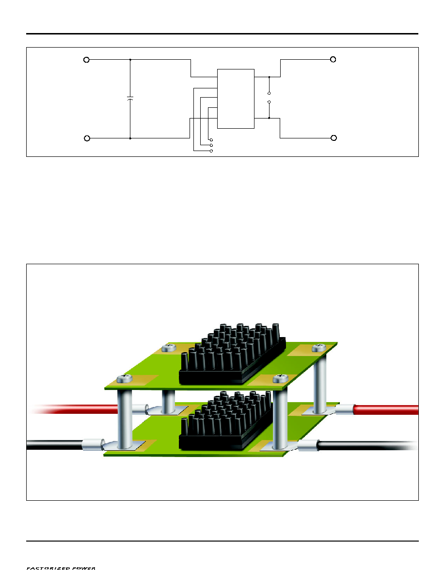
4. PARALLELING
The paralleling and current sharing capability of the devices
can be demonstrated by stacking multiple evaluation PCBs
and interconnecting the inputs and outputs with standoffs
of sufficient current handling capability to create a
3-dimensional array. See Figure 3.
5. INPUT CURRENT MEASUREMENT
A current probe can be passed around the +IN lead connected
to the V∑I Chip. Input capacitors on the evaluation board
are downstream of this measurement point.
V
∑
I C
HIP
TM
Evaluation Board
∑ Oscilloscope probe jack
for output voltage and
ripple measurements
∑ Simple to use
∑ Ring lug or solder connections
∑ Parallelable
∑ This board suitable for the
following V∑I Chip products:
Bus Converter Module (BCM)
Voltage Transformation
Module (VTM)
PRELIMIN
ARY
Vicor Corporation Tel: 800-735-6200 vicorpower.com V∑I Chip Evaluation Board Rev.
1.2 Page 2 - 4
4
5
Specifications
6. TEMPERATURE MONITOR (TM)
A DVM can be connected between TM (positive) and
SG (negative) to monitor the internal temperature of
the V∑I Chip.
7. PRIMARY CONTROL (PC)
The PC can be used to disable the V∑I Chip, monitor status,
or provide a primary referenced bias supply.
a.) Connecting PC to SG or to the ≠IN will disable
the V∑I Chip.
b.) Connecting a DVM or oscilloscope between PC
(positive) and SG or ≠IN (negative) will indicate the
status of the V∑I Chip. Please note that the V∑I Chip
does not have active current sinking capability.
c.) Connecting a load between PC (positive) and SG
or ≠IN (negative) will provide a primary referenced
bias supply.
8. EFFICIENCY MEASUREMENT
As the V∑I Chip can deliver and consume large currents, the
effect of the PCB must be considered when making an
efficiency measurement. Be certain to accurately measure
the voltage directly at the V∑I Chip using the appropriate
pair of contact points located at the corners of the V∑I Chip.
ORDERING INFORMATION:
The evaluation board is specified by suffixing "≠EB" to the
appropriate V∑I Chip model number that includes in-board
mounting and integral pin fin heatsink. See vicorpower.com for
model number listings.
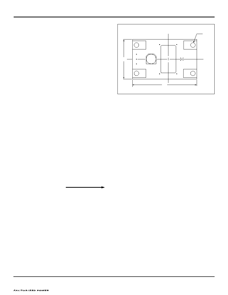
1.66
TM
SG
PC
+IN
≠IN
+OUT
≠ OUT
J1
CL
2.67
ÿ 0.20 Typ
Figure 1-- V∑I Chip demo board layout and dimensional drawing,
Component side. (Dimensions are in inches)
RECOMMENDED HARDWARE:
QTY
Description
Manufacturer Vicor
P/N
P/N
4
Ring Lug
PANDUIT LCAS6-10-L
4
#10-32 Screw
4
#10 Flat Washer
4
#10 Lock Washer
Kit # 26647
4
#10 Hex Nut
All hardware is Stainless Steel except Ring Lug.
Kit # 26647 included with evaluation board.
}
Vicor Corporation Tel: 800-735-6200 vicorpower.com V∑I Chip Evaluation Board Rev.
1.2 Page 3 - 4
4
5
Specifications, continued
+In
PC
SG
TM
≠In
+Out
≠Out
+OUT
≠OUT
C1
100
µF
63V
V∑I Chip
Output scope connector
≠IN
+IN
TM
SG
PC
Figure 2-- V∑I Chip evaluation board schematic
Figure 3-- Paralleling connections
+ OUT
≠ OUT
+ IN
≠ IN
PRELIMIN
ARY
THERMALS
For most lab environments a fan is not required as long as the
airflow around the device is unobstructed. The temperature
monitor function (TM) may be used to monitor the effective
junction temperature of the V∑I Chip.
CAUTION
The V∑I Chip and evaluation board can comfortably operate at
surface temperatures which may pose a thermal hazard to the
operator. Be careful not to touch any exposed surface. Certain
V∑I Chips may operate at potentially dangerous voltages, use
care in such cases. This evaluation PCB is not intended for use
in end item equipment.

Vicor Corporation Tel: 800-735-6200 vicorpower.com V∑I Chip Evaluation Board Rev.
1.2 Page 4 - 4
P/N
26692 9/29/10M
4
5
Vicor's comprehensive line of power solutions includes high density AC-DC
and DC-DC modules and accessory components, fully configurable AC-DC
and DC-DC power supplies, and complete custom power systems.
Information furnished by Vicor is believed to be accurate and reliable. However, no responsibility is
assumed by Vicor for its use. No license is granted by implication or otherwise under any patent or patent
rights of Vicor. Vicor components are not designed to be used in applications, such as life support systems,
wherein a failure or malfunction could result in injury or death. All sales are subject to Vicor's Terms and
Conditions of Sale, which are available upon request.
Specifications are subject to change without notice.
Vicor Corporation
25 Frontage Road
Andover, MA, USA 01810
Tel: 800-735-6200
Fax: 978-475-6715
Email
Vicor Express: vicorexp@vicr.com
Technical Support: apps@vicr.com
Intellectual Property
Vicor and its subsidiaries own Intellectual Property (issued U.S. and Foreign Patents and
pending patent applications) relating to the product described in this data sheet including;
∑ The electrical and thermal utility of the V∑IChip package
∑ The design of the V∑IChip package
∑ The Power Conversion Topology utilized in the V∑IChip package
∑ The Control Architecture utilized in the V∑IChip package
∑ The Factorized Power Architecture.
Purchase of this product conveys a license to use it. Anybody wishing to utilize Vicor
proprietary technologies must first obtain a license. Potential users are encouraged to first
contact Vicor Intellectual Property Department.