 | –≠–ª–µ–∫—Ç—Ä–æ–Ω–Ω—ã–π –∫–æ–º–ø–æ–Ω–µ–Ω—Ç: QPI-2L | –°–∫–∞—á–∞—Ç—å:  PDF PDF  ZIP ZIP |
Picor Corporation ∑ www.picorpower.com
QPI-2L Data Sheet Rev. 2.0 Page 1 of 8
Features
∑ >55 dB CM attenuation at 250 kHz
∑ >70 dB DM attenuation at 250 kHz
∑ 40 Vdc (max input)
∑ 12 Amp rating
∑ 100 Vdc surge 100 ms
∑ 707 Vdc Hi-pot hold off to Shield Plane
∑ 1.0" x 1.0" x 0.2" SiP (System-in-Package)
∑ SMT Land Grid Array (LGA)
∑ -40∞ to +100∞C PCB temperature (See Fig. 5)
∑ Active filtering reduces volume and height
∑ Efficiency 99% at full load
∑ Connect in series for higher attenuation
∑ TÐV approved
Applications
∑ Industrial bus supplies
∑ Telecom base stations
∑ COTS systems
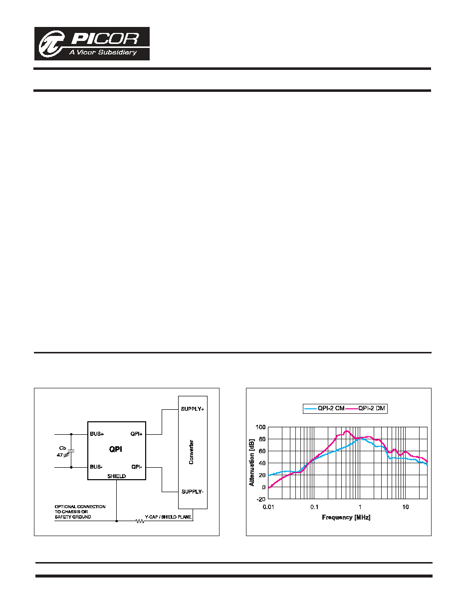
Typical Application
QPI Performance
RY=10
, 1/4 W
Figure 1 - QPI-2 circuit on input bus.
Figure 2 - Attenuation curves showing common-mode and
differential-mode attenuation.
Description
The QPI-2 active EMI filter attenuates conducted
common-mode (CM) and differential-mode (DM) noise
over the CISPR22 frequency range of 150 kHz to 30
MHz. The product is designed for use on a 24 Vdc bus
(10-40 Vdc). The QPI-2's 12 A rating supports multiple
DC-DC converter loads up to a PCB temperature of
60∞C. At a 100∞C PCB temperature the QPI-2 supports
10 A loads. Designed for a nominal 24 V bus, the QPI-2
supports industrial and COTS applications.
In comparison to passive solutions, the use of active
filtering reduces the volume of the common-mode
choke, providing a low profile, surface mount device.
Smaller size saves valuable board real estate and the
reduced height enhances airflow in blade applications.
The QPI-2 is available in a 1.0" x 1.0" x 0.2" SiP (System
in Package) with LGA mounting. QPI-2-EVAL1 kits are
available for testing the QPI-2. The evaluation board
has a mounted QPI-2 with screw terminals for quick
in-circuit testing.
Check picorpower.com for the QPI-2-EVAL1 evaluation
board and the QPI-AN1 Application Note.
QPI-2L
QuietPower
TM
12 Amp Active EMI Filter for 24 V DC Bus
Æ
Picor Corporation ∑ www.picorpower.com
QPI-2L Data Sheet Rev. 2.0 Page 2 of 8
Absolute Maximum Ratings
≠
Exceeding these parameters may result in permanent damage to the product.
Electrical Characteristics
≠
Parameter limits apply over the operating temp. range unless otherwise noted.
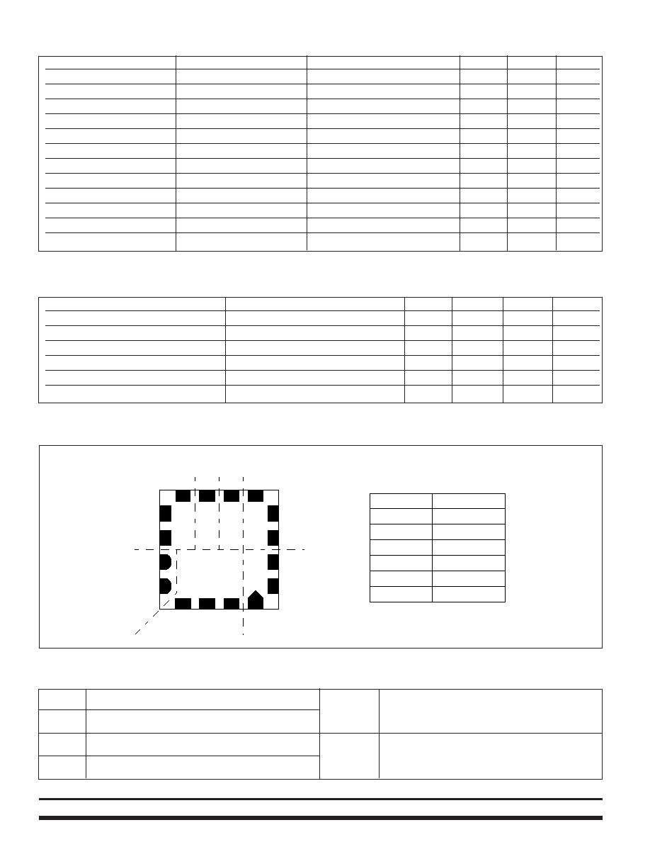
Pins
Parameter
Notes
Min
Max
Units
BUS+ to BUS-
Input voltage
Continuous
-0.5
40
Vdc
BUS+ to BUS-
Input voltage
100ms transient
-0.5
100
Vdc
BUS+/BUS- to Shield Plane
BUS inputs to Shield Hipot
Per test std.
+/-500
Vdc
QPI+ to QPI-
Input to output current
Continuous @ 25∞C
12
Adc
Package
Power dissipation
V
BUS
= 24 V, I
BUS
= 12 Adc, 25∞C
4.0
W
Package
Operating temperature
PCB to QPI Interface
-40
100
∞C
Package
Thermal resistance
Free air
50
∞C/W
Package
Junction temperature
Internal @ Pdmax and 15∞C/W
160
∞C
Package
Thermal resistance
PCB layout (see Figs. 9 & 10)
1
15
∞C/W
Package
Storage temperature
-40
125
∞C
Package
Re-flow temperature
20 second exposure @
212
∞C
All Pins
ESD
HBM
+/-2
kV
Parameter
Notes
Min
Typ
Max
Units
BUS+ to BUS- input range
Measured at 10 A
2
10
40
Vdc
BUS+ to QPI+ voltage drop
Measured at 10 A
2
-300
mVdc
BUS- to QPI- voltage drop
Measured at 10 A
2
20
mVdc
Common-mode insertion loss
V
BUS
= 24 V frequency = 500 kHz
60
dB
Differential-mode insertion loss
V
BUS
= 24 V frequency = 500 kHz
85
dB
Input bias current at 40 Volts
Input current from BUS+ to BUS-
17
mA
Note 1 - Refer to Figures 9 & 10 for PCB layout guidelines to achieve this thermal resistance when re-flowed onto the PCB.
Pad Designations
BUS+
BUS-
QPI+
QPI-
THERM 1
SHIELD
THERM 2
12,13,14
1,15,16
7,8,9
2,3,4
10
5,6
11
BUS-
BUS+
QPI+
SHIELD
THERM 1
THERM 2
7
8
9
11
12
13
16
10
14
15
1
2
3
4
5
6
QPI-
Pad Description
BUS-
Negative bus potential
BUS+
Positive bus voltage
QPI-
Negative input to the converter
QPI+
Positive input to the converter
THERM1
Internal connection must be electrically
THERM2
floating but maximize copper landing
for heat sinking.
Shield
The shield connects to the converter
shield and Y-capacitor common point
through RY.
Note 2 - Refer to Figure 5 for current derating curve.
QPI-2: (bottom view)
Picor Corporation ∑ www.picorpower.com
QPI-2L Data Sheet Rev. 2.0 Page 3 of 8
Applications Information
The QPI-2 is an active EMI filter providing conducted
common-mode and differential-mode attenuation
from 150 kHz to 30 MHz. The QPI-2 attenuates noise at
all frequencies covered by EN55022. Designers should
be aware that to select and qualify an EMI filter they
must test the filter in their equipment under the set up
and conditions specified in the EMI standards that they
are trying to meet.
Filter performance is highly dependent on several
factors and cannot be derived from the attenuation
curves shown in Figure 2 alone. Performance is a
complex function of filter element impedances and
noise source impedances, which vary in magnitude and
phase over the frequency spectrum. Measurements
should be made in consultation with in-house
compliance testing or an independent EMI test facility.
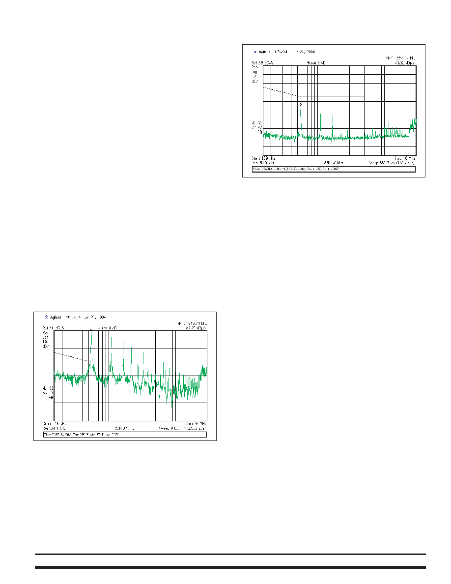
Test Example
Figures 3 and 4 show the before and after plots of a
DC-DC converter noise profile to demonstrate the
performance of the QPI-2. The plots were taken using
the standard measurement technique and set up defined
in CISPR22. The results show the total noise spectrum
for a standard DC-DC converter under load compared
to the EN55022 Class B Quasi-peak detection limit.
The resulting plot in Figure 4 shows the QPI-2 is
effective in reducing the total conducted noise
spectrum measured pre-filter to well below the
EN55022 Class B Quasi-peak detection limit.
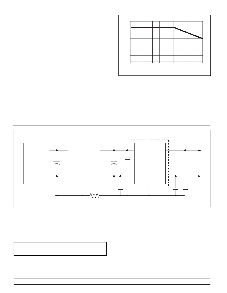
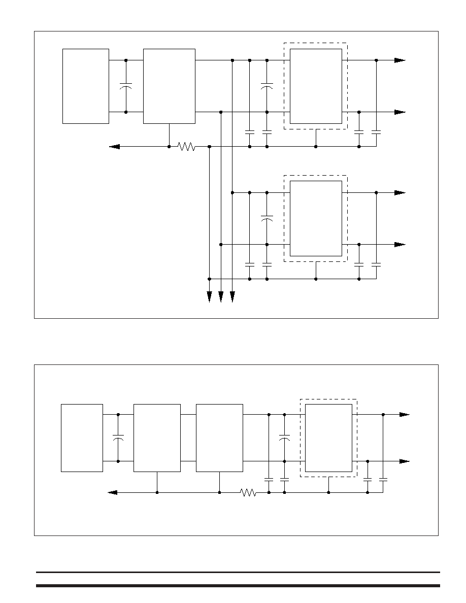
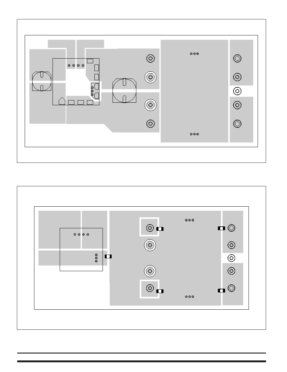
Layout and Circuit
Application of the QPI-2 requires PCB layout practices
similar to those used with passive EMI filters. The circuit
in Figure 6 and the PCB layout in Figures 9 & 10 should
be used as a design guide to ensure successful
application of the QPI-2. Refer to the application note
QPI- AN1 for additional PCB layout recommendations.
Note: For optimum performance of the QPI-2 it is
critical to connect the QPI-2 Shield Plane (pins 5 & 6) to
the converter EMI Shield Plane (common point of C1-
C4"Y" capacitors) thru RY as shown in Figure 6. If the
safety earth-ground connection (chassis or case) is
connected in the power conversion section of the PCB
it should be at the input bus of the QPI-2 Shield Plane,
shown as the optional connection in Figure 6.
Connecting the converter EMI shield plane directly to
chassis ground may degrade the QPI-2 attenuation
performance. The typical value for RY is 10 Ohms. The
recommended part is a 5% tolerance SMT1206 or
similarly rated 0.25 W through-hole resistor.
QPIs will filter multiple DC-DC converters up to the
maximum current rating. The schematic in Figure 7
shows the required circuit for multiple DC-DC
converters. The Shield Plane should be added under
each converter as a common EMI Shield. Note that only
a single RY is required in a multiple converter
configuration.
Figure 3 ≠ Conducted EMI profile of a DC-DC Converter
without filter.
Figure 4 ≠ Conducted EMI profile of a DC-DC Converter
with QPI-2.
Picor Corporation ∑ www.picorpower.com
QPI-2L Data Sheet Rev. 2.0 Page 4 of 8
Figure 6 ≠ Recommended schematic for QPI. Values of C
IN
and C1-C4 should be the values recommended by the converter manufacturer.
If the manufacturer does not specify a value for the Y-capacitors use 4.7nF. Ry=10, 1/4 W.
Part Number
Description
QPI-2L
QPI-2 Land Grid Array
Ordering Information
BUS+
QPI+
BUS-
QPI-
SHIELD
BUS
SUPPLY
QPI
V
IN
+
V
OUT
+
V
IN
-
V
OUT
-
SHIELD
CONVERTER
Optional Connection
C1
C2
C3
C4
RY
PCB plane under converter
C
IN
CB
47µF
If higher attenuation is required, QPIs can be
connected in series. Figure 8 shows the proper
schematic for QPIs in series. Note that only one RY is
required in this configuration.
The QPI can also be used to filter embedded or "down"
converters made up of discrete components. Where
ever possible a Shield Plane and Y-capacitor decoupling
should be included in the embedded converter design.
Follow the circuit and layout recommendations for a
brick converter shown in Figures 7, 9 & 10.
Thermal Considerations
The current derating curve shown in Figure 5 should be
used when the PCB temperature in close proximity of
the QPI-2 exceeds 60∞C. For example, the QPI-2 will
support up to 10 A of current or 280 W from a 28 Vdc
bus at an 80∞C interface temperature. Temperature
should be measured at the PCB interface to the QPI-2
on the Bus +/- pads or the QPI+/- pads. Refer to Figures
9, 10 & 12 for PCB layout recommendation.
0
10
20
30
40
50
60
70
80
90
100
PCB to QPI Interface Temperature (Deg. C)
QPI Current (A)
14
12
10
8
6
4
2
0
Figure 5 ≠ QPI-2 current derating curve.
Picor Corporation ∑ www.picorpower.com
QPI-2L Data Sheet Rev. 2.0 Page 5 of 8
Figure 7 ≠ Schematic for supporting multiple DC-DC converters. Note only a single RY is required. Use values recommended by converter
manufacturer for C
IN
and Y-capacitors C1-C8.
BUS
SUPPLY
V
IN
+
V
OUT
+
V
IN
-
V
OUT
-
SHIELD
CONVERTER
Optional Connection
C2
C3
C4
RY
PCB plane under converter
C
IN
1
BUS+
QPI+
BUS-
QPI-
SHIELD
QPI
CB
47
µF
C1
V
IN
+
V
OUT
+
V
IN
-
V
OUT
-
SHIELD
CONVERTER
C6
C7
C8
PCB plane under converter
C
IN
2
C5
Additional Converters
10
, 1/4 W
Figure 8 ≠ Series connection of QPI for higher attenuation.
BUS+
QPI+
BUS-
QPI-
SHIELD
BUS
SUPPLY
QPI
V
IN
+
V
OUT
+
V
IN
-
V
OUT
-
SHIELD
CONVERTER
Optional Connection
C2
C3
C4
RY
PCB plane under converter
C
IN
BUS+
QPI+
BUS-
QPI-
SHIELD
QPI
CB
47 µF
C1
10
, 1/4 W
Picor Corporation ∑ www.picorpower.com
QPI-2L Data Sheet Rev. 2.0 Page 6 of 8
RY
C1
C2
C4
C3
Bottom Layer - Top View
Shield Plane
Thermal 1
Thermal 2
QPI Shield
CB
C
IN
Top Layer - Top View
Thermal 1
Thermal 2
Shield Plane
C
onverter
+
+
Out
-
Out
C
onverter
-
*
*
*
*
*
+
+
Figure 9 ≠ Recommended layout for top layer of PCB. Pattern shows optional pins (*) dependent on converter used in design.
(Actual size with half brick footprint)
Figure 10 ≠ Recommended layout for bottom layer of PCB. Note location of RY.
Picor Corporation ∑ www.picorpower.com
QPI-2L Data Sheet Rev. 2.0 Page 7 of 8
0.000
0.100
0.300
0.492 0.441
0.441
0.100
0.300
0.492
0.000
0.100
0.300
0.492
0.400
0.441
0.441
0.400
0.100
0.300
0.492
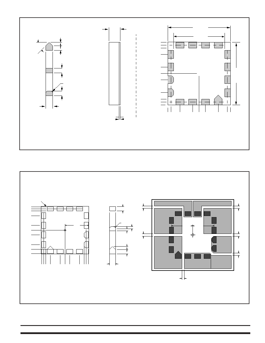
QPI SIP Package
(Bottom View)
0.9843
0.8000
0.9843
0.0200
0.1773
13 places
2 places
45.000∞
0.1250
0.0820
0.0625
0.0820
0.0820
R0.0410
0.1310
0.0880
0.0655
0.0440
0.0440
0.0880
2 places
13 places
0.0000
0.1000
0.3000
0.1000
0.3000
0.3970
0.3970
0.4410
0.4410
0.4850
0.4850
0.0000
0.1000
0.3000
0.4410
0.3970
0.4850
0.0000
0.1000
0.3000
0.3970
0.4850
QPI Package Outline
QPI PCB Pad Pattern
(Top View)
R0.0440
BUS-
BUS+
QPI+
SHIELD
QPI-
THERM 1
THERM 2
0.4410
0.050
0.050
0.050
0.050
0.050
0.050
0.4410
0.492
Figure 11 ≠ QPI package dimensions and pad locations.
Figure 12 ≠Recommended PCB layout pattern. Use 1.3mm clearance around shield pads 5 & 6 to adjacent lands. See Figures 9 & 10 for
recommended connection layouts.

Picor Corporation ∑ www.picorpower.com ∑ QPI-2L Data Sheet
P/N 27779 Rev. 2.0
10/04/10M
Vicor's comprehensive line of power solutions includes high-density AC-DC & DC-DC modules
and accessory components, fully configurable AC-DC & DC-DC power supplies, and complete
custom power systems.
Information furnished by Vicor is believed to be accurate and reliable. However, no responsibility is
assumed by Vicor for its use. No license is granted by implication or otherwise under any patent or patent
rights of Vicor. Vicor components are not designed to be used in applications, such as life support
systems, wherein a failure or malfunction could result in injury or death. All sales are subject to Vicor's
Terms and Conditions of Sale, which are available upon request.
Specifications are subject to change without notice.
Vicor Corporation
25 Frontage Road, Andover, MA, USA 01810
Tel: 800-735-6200 Fax: 978-475-6715
Email
Vicor Express: vicorexp@vicr.com
Technical Support: apps@vicr.com