∑ 125∞C operation
∑ 1 µs transient response
∑ >3.5 million hours MTBF
∑ Typical efficiency 93% at 1.5 V/50 A
∑ No output filtering required
∑ BGA or J-Lead packages
Vicor Corporation
Tel: 800-735-6200 V∑I Chip Voltage Transformation Module V048K015T090 Rev. 1.0 Page 1 of 16
vicorpower.com
PRELIMIN
ARY
Product Description
The V048K015T090 V
∑
I Chip Voltage Transformation
Module (VTM) breaks records for speed, density and
efficiency to meet the demands of advanced DSP,
FPGA, ASIC, processor cores and microprocessor
applications at the point of load (POL) while providing
isolation from input to output. It achieves a response
time of less than 1 µs and delivers up to 90 A in a
volume of less than 0.25 in
3
while providing low output
voltages with unprecedented efficiency. It may be
paralleled to deliver hundreds of amps at an output
voltage settable from 0.8 to 1.7 Vdc.
The VTM V048K015T090's nominal output voltage is
1.5 Vdc from a 48 Vdc input factorized bus, V
f
, and is
controllable from 0.8 to 1.7 Vdc at no load, and from
0.8 to 1.6 Vdc at full load, over a V
f
input range of 26
to 55 Vdc. It can be operated either open- or closed-loop
depending on the output regulation needs of the
application. Operating open-loop, the output voltage
tracks its V
f
input voltage with a transformation ratio,
K = 1/32, and an output resistance, R
OUT
= 1.0 milliohm, to
enable applications requiring a programmable low
output voltage at high current and high efficiency.
Closing the loop back to an input Pre-Regulation
Module (PRM) or DC-DC converter can compensate
for R
OUT
.
The 1.5 V VTM achieves break-through current density
of 360 A/in
3
in a V
∑
I Chip package compatible with
standard pick-and-place and surface mount assembly
processes. The V
∑
I Chip BGA package supports in-board
mounting with a low profile of 0.16" (4 mm) over the
board. A J-lead package option supports on-board
surface mounting with a profile of only 0.25" (6 mm)
over the board. The VTM's fast dynamic response and
low noise eliminate the need for bulk capacitance at the
load, substantially increasing the POL density while
improving reliability and decreasing cost.
Absolute Maximum Ratings
Parameter
Values
Unit
Notes
+In to -In
-1.0 to 60.0
Vdc
+In to -In
100
Vdc
For 100 ms
PC to -In
-0.3 to 7.0
Vdc
TM to -In
-0.3 to 7.0
Vdc
VC to -In
-0.3 to 19.0
Vdc
+Out to -Out
-0.1 to 4.0
Vdc
Isolation voltage
2,250
Vdc
Input to Output
Operating junction temperature
-40 to 125
∞C
See Note
Output current
90
A
Continuous
Peak output current
135
A
For 1 ms
Case temperature during reflow
208
∞C
Storage temperature
-40 to 150
∞C
Output power
145
W
Continuous
Peak output power
217
W
For 1 ms
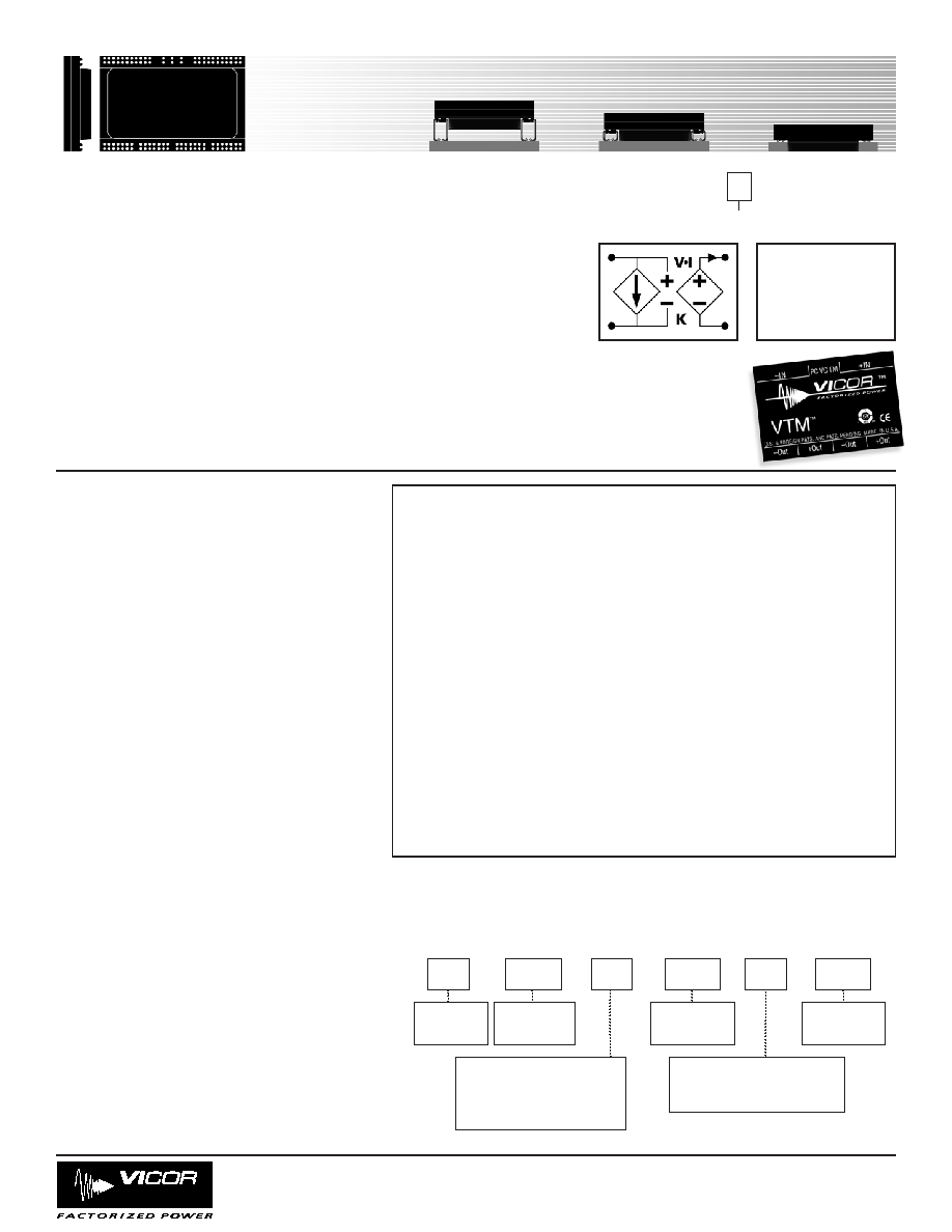
V∑I Chip
TM
≠ VTM
Voltage Transformation Module
∑ 48 V to 1.5 V V∑I Chip Converter
∑ 90 A (135 A for 1 ms)
∑ High density ≠ 360 A/in
3
∑ Small footprint ≠ 84 A/in
2
∑ Low weight ≠ 0.5 oz (14 g)
∑ Pick & Place / SMD
V048K015T090
V
f
= 26 - 55 V
V
OUT
= 0.8 - 1.7 V
I
OUT
= 90 A
K = 1/32
R
OUT
= 1.2 m
max
Actual size
©
VTM
Note:
The referenced junction is defined as the semiconductor having the highest temperature.
This temperature is monitored by the temperature monitor (TM) signal and by a shutdown comparator.
K indicates BGA configuration. For other
mounting options see Part Numbering below.
Output Current
Designator
(=I
OUT
)
V
048
K
015
T
090
Voltage
Transformation
Module
Input Voltage
Designator
Product Grade Temperatures (∞C)
Grade
Storage
Operating
T
-40 to150
-40 to125
Configuration Options
A = On-board, elevated (Fig.16)
F = On-board (Fig.15)
K = In-board (Fig.14)
Output Voltage
Designator
(=V
OUT
x10)
Part Numbering

Vicor Corporation
Tel: 800-735-6200 V∑I Chip Voltage Transformation Module V048K015T090 Rev. 1.0 Page 2 of 16
vicorpower.com
PRELIMIN
ARY
Specifications
Parameter
Min
Typ
Max
Unit
Note
Input voltage range
26
48
55
Vdc
Operable down to zero V with external bias voltage
Input dV/dt
1
V/µs
Input overvoltage turn-on
57.6
Vdc
Input overvoltage turn-off
59.0
Vdc
Input current
3.2
Adc
Input reflected ripple current
135
mA p-p
Using test circuit in Fig.17; See Fig.1
No load power dissipation
2.50
3.5
W
Internal input capacitance
4
µF
Internal input inductance
20
nH
INPUT (Conditions are at 48 Vin, full load, and 25∞C ambient unless otherwise specified)
Parameter
Min
Typ
Max
Unit
Note
Rated DC current
0
90
Adc
Peak repetitive current
135
A
Max pulse width 1ms, max duty cycle 10%,
baseline power 50%
DC current limit
92
108
126
Adc
Current share accuracy
5
10
%
See Parallel Operation on page 10
Efficiency
Half load
92.5
93.4
%
See Fig.3, 1.5 Vout
Full load
91.0
91.5
%
See Fig.3, 1.5 Vout
Internal output inductance
1.6
nH
Internal output capacitance
306
µF
Effective value
Load capacitance
100,000
µF
Output overvoltage setpoint
1.80
Vdc
Output ripple voltage
No external bypass
62
110
mV
See Figs.2 and 5
200 µF bypass capacitor
2
mV
See Fig.6
Effective switching frequency
2.4
2.5
2.6
MHz
Fixed, 1.25 MHz per phase
Line regulation
K
0.0309
1/32
0.0316
V
OUT
= K∑V
IN
at no load
Load regulation
R
OUT
1.0
1.2
m
See Fig.20
Transient response
Voltage overshoot
20
mV
90 A load step with 100 µF C
IN;
See Figs.7 and 8
Response time
200
ns
See Figs.7 and 8
Recovery time
1
µs
See Figs.7 and 8
OUTPUT (Conditions are at 48 Vin, full load, and 25∞C ambient unless otherwise specified)
Vicor Corporation
Tel: 800-735-6200 V∑I Chip Voltage Transformation Module V048K015T090 Rev. 1.0 Page 3 of 16
vicorpower.com
Specifications
Figure 1-- Input reflected ripple current at full load and 48 Vin
Output Current (A)
Efficiency vs. Output Current
Efficiency (%)
75
77
79
81
83
85
87
89
91
93
95
0
10
20
30
40
50
60
70
80
90
1.6V
1.5V
1.2V
1.0V
0.8V
Figure 3-- Efficiency vs. output current and output voltage
Output Current (A)
Power Dissipation vs. Output Current
Power Dissipation (W)
0
1
2
3
4
5
6
7
8
9
10
11
12
13
14
0
10
20
30
40
50
60
70
80
90
0.8V
1.0V
1.2V
1.5V
Figure 4--Power dissipation as a function of output current and
output voltage
WAVEFORMS
Figure 6--Output voltage ripple at full load and 1.5 Vout with
200 µF ceramic external bypass capacitance and 20 nH
distribution inductance.
Figure 5-- Output voltage ripple at full load and 1.5 Vout;
without any external bypass capacitor.
Output Ripple vs Load
Output Ripple (mV)
0
5
10
15
20
25
30
35
40
45
50
55
60
65
0
10
20
30
40
50
60
70
80
90
Output Current (A)
Figure 2-- Output voltage ripple vs. output current at 1.5 Vout
with no POL bypass capacitance.

Vicor Corporation
Tel: 800-735-6200 V∑I Chip Voltage Transformation Module V048K015T090 Rev. 1.0 Page 4 of 16
vicorpower.com
PRELIMINARY
Parameter
Min
Typ
Max
Unit
Note
Primary Control (PC)
DC voltage
4.8
5.0
5.2
Vdc
Module disable voltage
2.4
2.5
Vdc
Module enable voltage
2.5
2.6
Vdc
Current limit
2.4
2.5
2.9
mA
Source only
Disable delay time
4
10
µs
PC low to Vout low
Temperature Monitor (TM)
27∞C setting
3.00
Vdc
Operating junction temperature
Temperature coefficient
10
mV/∞C
Full range accuracy
±5
∞C
Operating junction temperature
Current limit
100
µA
Source only
VTM Control (VC)
External boost voltage
12.0
14.0
19.0
Vdc
Required for VTM start up without PRM
External boost duration
10
ms
Vin must be >26 V for VTM to remain operating
without boost voltage.
Specifications, continued
Auxiliary Pins (Conditions are at 48 Vin, full load, and 25∞C ambient unless otherwise specified)
Parameter
Min
Typ
Max
Unit
Note
MTBF
MIL-HDBK-217F
3.5
Mhrs
25∞C, GB
Isolation specifications
Voltage
2,250
Vdc
Input to Output
Capacitance
2,500
pF
Input to Output
Resistance
10
M
Input to Output
Agency approvals (pending)
cTÐVus
UL/CSA 60950, EN 60950
CE Mark
Low voltage directive
Mechanical parameters
See mechanical drawing, Figs.10 and 12
Weight
0.5 / 14.0
oz / g
Dimensions
Length
1.26 / 32
in / mm
Width
0.85 / 21.5
in / mm
Height
0.23 / 5.9
in / mm
GENERAL
Figure 7-- 0-90 A step load change with 100 µF input
capacitance and no output capacitance.
Figure 8-- 90-0 A step load change with 100 µF input
capacitance and no output capacitance.
Vicor Corporation
Tel: 800-735-6200 V∑I Chip Voltage Transformation Module V048K015T090 Rev. 1.0 Page 5 of 16
vicorpower.com
PRELIMIN
ARY
Specifications, continued
V∑I CHIP STRESS DRIVEN PRODUCT QUALIFICATION PROCESS
Symbol
Parameter
Min
Typ
Max
Unit
Note
Over temperature shutdown
125
130
135
∞C
Junction temperature
Thermal capacity
0.61
Ws/∞C
R
JC
Junction-to-case thermal impedance
1.1
∞C/W
R
JB
Junction-to-BGA thermal impedance
2.1
∞C/W
R
JA
Junction-to-ambient
1
6.5
∞C/W
R
JA
Junction-to-ambient
2
5.0
∞C/W
THERMAL
Notes
1. V048K015T090 surface mounted in-board to a 2" x 2" FR4 board, 4 layers 2 oz Cu, 300 LFM.
2. V048K015T090 with optional 0.25"H Pin Fins surface mounted on FR4 board, 300 LFM.
Test
Standard
Environment
High Temperature Operational Life (HTOL)
JESD22-A-108-B
125∞C, Vmax, 1,008 hrs
Temperature cycling
JESD22-A-104B
-55∞C to 125∞C, 1,000 cycles
High temperature storage
JESD22-A-103A
150∞C, 1,000 hrs
Moisture resistance
JESD22-A113-B
Moisture sensitivity Level 5
Temperature Humidity Bias Testing (THB)
EIA/JESD22-A-101-B
85∞C, 85% RH, Vmax, 1,008 hrs
Pressure cooker testing (Autoclave)
JESD22-A-102-C
121∞C, 100% RH, 15 PSIG, 96 hrs
Highly Accelerated Stress Testing (HAST)
JESD22-A-110B
130∞C, 85% RH, Vmax, 96 hrs
Solvent resistance/marking permanency
JESD22-B-107-A
Solvents A, B & C as defined
Mechanical vibration
JESD22-B-103-A
20g peak, 20-2,000 Hz, test in X, Y & Z directions
Mechanical shock
JESD22-B-104-A
1,500g peak 0.5 ms pulse duration, 5 pulses in 6 directions
Electro static discharge testing ≠ human body model
EIA/JESD22-A114-A
Meets or exceeds 2,000 Volts
Electro static discharge testing ≠ machine model
EIA/JESD22-A115-A
Meets or exceeds 200 Volts
Highly Accelerated Life Testing (HALT)
Per Vicor Internal
Operation limits verified, destruct margin determined
Test Specification*
Dynamic cycling
Per Vicor internal
Constant line, 0-100% load, -20∞C to 125∞C
test specification*
* For details of the test protocols see Vicor's website.
Test
Standard
Environment
BGA solder fatigue evaluation
IPC-9701
Cycle condition: TC3 (-40 to +125∞C)
IPC-SM-785
Test duration: NTC-B (500 failure free cycles)
Solder ball shear test
IPC-9701
Failure through bulk solder or copper pad lift-off
V∑I CHIP BALL GRID ARRAY INTERCONNECT QUALIFICATION