vicorpower.com
800-735-6200
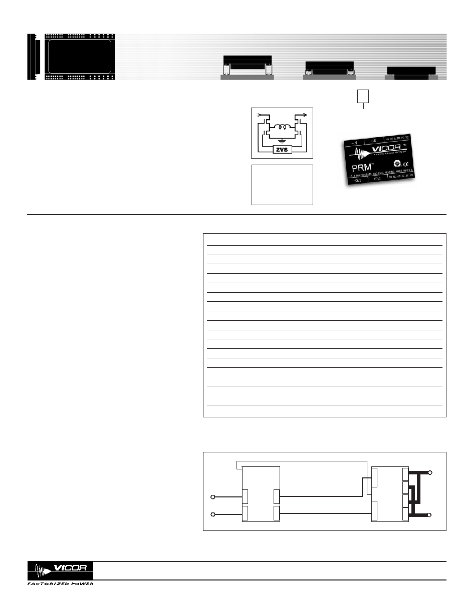
V∑I Chip Pre-Regulator Module
P048K048T24AL
Rev. 1.4
Page 1 of 15
PRELIMINARY
∑ 48 V input V∑I Chip PRM
∑ Vin range 36 ≠ 75 Vdc
∑ High density ≠ 1000 W/in
3
∑ Small footprint ≠ 250 W/in
2
∑ Low weight ≠ 0.5 oz (14 g)
∑ Adaptive Loop feedback
∑ ZVS buck-boost regulator
∑ 1.5 MHz switching frequency
∑ 96% Efficiency
∑ 125∞C operation
P048K048T24AL
Vin = 36 ≠ 75 V
V
f
= 26 ≠ 55 V
P
f
= 240 W
I
f
= 5 A
©
V∑I Chip
TM
≠ PRM-AL
Pre-Regulator Module
K indicates BGA configuration. For other mounting
options see Part Numbering on Page 2.
Product Description
The V∑I Chip Pre-Regulator Module (PRM) is a very
efficient non-isolated regulator capable of both
boosting and bucking a wide range input voltage. It is
specifically designed to provide a controlled Factorized
Bus distribution voltage for powering downstream
V∑I Chip Voltage Transformation Modules (VTMs) --
fast, efficient, isolated low noise Point-of-Load (POL)
converters. In combination, PRMs and VTMs form a
complete DC-DC converter subsystem offering all of
the unique benefits of Vicor's Factorized Power
Architecture (FPA): high density and efficiency; low
noise operation; architectural flexibility; extremely fast
transient response; and elimination of bulk capacitance
at the Point-of-Load (POL).
In FPA systems, the POL voltage is the product of the
Factorized Bus voltage delivered by a PRM and the
"K-factor" (the fixed voltage transformation ratio) of a
downstream VTM. The PRM controls the Factorized Bus
voltage to provide regulation at the POL. Because VTMs
perform true voltage division and current multiplication,
the Factorized Bus voltage may be set to a value that is
substantially higher than the bus voltages typically
found in "intermediate bus" systems, reducing
distribution losses and enabling use of narrower
distribution bus traces. A PRM-VTM chip set can
provide up to 100 A, or 230 W, at a FPA system density
of 200 A/in
3
, or 460 W/in
3
-- and because the PRM
can be located, or "factorized," remotely from the
POL, these power densities can effectively be doubled.
The PRM described in this data sheet features a unique
"Adaptive Loop" compensation feedback: a single wire
alternative to traditional remote sensing and feedback
loops that enables precise control of an isolated POL
voltage without the need for either a direct connection
to the load or for noise sensitive, bandwidth limiting,
isolation devices in the feedback path.
Actual size
Parameter
Values
Unit
+In to -In
-1.0 to 85.0
Vdc
PC to -In
-0.3 to 6.0
Vdc
PR to -In
-0.3 to 9.0
Vdc
IL to -In
-0.3 to 6.0
Vdc
VC to -In
-0.3 to 18.0
Vdc
+Out to -Out
-0.3 to 59
Vdc
SC to -Out
-0.3 to 3.0
Vdc
VH to -Out
-0.3 to 9.5
Vdc
OS to -Out
-0.3 to 9.0
Vdc
CD to -Out
-0.3 to 9.0
Vdc
SG to -Out
100
mA
Continuous output current
5
Adc
Continuous output power
240
W
Operating junction temperature
(M-Grade)
-55 to 125
∞C
(T-Grade)
-40 to 125
∞C
Storage temperature
(M-Grade)
-65 to 150
∞C
(T-Grade)
-40 to 150
∞C
Case temperature during reflow:
208
∞C
-In
PC
VC
TM
+In
-Out
+Out
VTM
+Out
-Out
K
Ro
+Out
≠Out
+In
≠In
VC
PC
TM
IL
VH
PR
NC
SG
SC
PRM-AL
OS
NC
CD
Factorized
Bus (V
f
)
Vin
Vout
The P048K048T24AL is used with any 048 input series VTM to provide a regulated and
isolated output.
DC-DC Converter
Absolute Maximum Ratings
PRM
vicorpower.com
800-735-6200
V∑I Chip Pre-Regulator Module
P048K048T24AL
Rev. 1.4
Page 2 of 15
PRELIMINARY
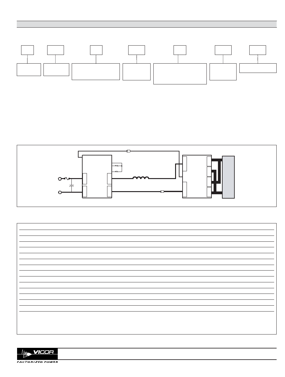
Overview of Adaptive Loop Compensation
Adaptive Loop compensation, illustrated in Figure 1, contributes to
the bandwidth and speed advantage of Factorized Power. The PRM
monitors its output current and automatically adjusts its output
voltage to compensate for the voltage drop in the output
resistance of the VTM. R
OS
sets the desired value of load voltage,
Vout; R
CD
is set to a value that compensates for the output
resistance of the VTM (which, ideally, is located at the point of
load). For selection of R
OS
and R
CD
, refer to Table 1 or Page 9.
The V∑I Chip's bi-directional VC port :
1. Provides a wake up signal from the PRM to the VTM that
synchronizes the rise of the VTM output voltage to that of the PRM.
2. Provides feedback from the VTM to the PRM to enable the PRM
to compensate for the voltage drop in VTM output resistance, R
O
.
-In
PC
VC
TM
+In
-Out
+Out
VTM
+Out
-Out
K
Ro
+Out
≠Out
+In
≠In
VC
PC
TM
IL
VH
PR
NC
SG
SC
PRM-AL
OS
NC
CD
L
O
A
D
Factorized
Bus (V
f
)
Vo = V
L ±
1.0%
(Io∑Ro)
K
V
f
=
V
L
+
K
Vin
R
OS
R
CD
Output Power
Designator
(=P
f
/10)
P
048
K
048
T
24
AL
Pre-Regulator
Module
Input Voltage
Designator
Product Grade Temperatures (∞C)
Grade
Storage
Operating
T
-40 to150 -40 to125
M
-65 to150 -55 to125
Configuration Options
F = Onboard (Fig.22)
K = Inboard (Fig.21)
Nominal
Factorized Bus
Voltage
AL = Adaptive Loop
Desired Load Voltage (Vdc)
VTM P/N
(1)
Max VTM Output Current (A)
(2)
R
OS
(k)
(3)
R
CD
()
(3)
1.0
V048K015T100
100
3.57
26.1
1.2
V048K015T100
100
2.94
32.4
1.5
V048K015T090
90
2.37
39.2
1.8
V048K020T080
80
2.61
35.7
2.0
V048K020T080
80
2.37
39.2
3.3
V040K033T060
60
2.15
43.2
5.0
V048K060T040
40
2.87
33.2
10
V048K120T025
25
2.26
41.2
12
V048K120T025
25
2.37
39.2
15
V048K160T019
18.8
2.49
37.4
24
V048K240T012
12.5
2.37
39.2
28
V048K320T009
9.4
2.74
35.7
36
V048K480T006
6.3
3.16
30.1
48
V048K480T006
6.3
2.37
39.2
Table 1 -- Configure your Chip Set using the PRM-AL
Note:
(1) Verify the configuration option and product grade temperature before ordering as shown above.
(2) See "PRM output power vs. VTM output power" on Page 10
(3) 1% precision resistors recommended
Figure 1 -- With Adaptive Loop control the output of the VTM is regulated over the load current range with only a single interconnect between the PRM and
VTM and without the need for isolation in the feedback path.
General Specifications
V∑I Chip Pre-Regulator Module
Part Numbering
vicorpower.com
800-735-6200
V∑I Chip Pre-Regulator Module
P048K048T24AL
Rev. 1.4
Page 3 of 15
PRELIMINARY
Parameter
Min
Typ
Max
Unit
Note
Input voltage range
36
48
75
Vdc
Input dV/dt
1
V/µs
Input undervoltage turn-on
33.8
35.3
Vdc
Input undervoltage turn-off
30.5
31.8
Vdc
Input overvoltage turn-on
75.8
77.3
Vdc
Input overvoltage turn-off
78.8
81.0
Vdc
Input quiescent current
0.5
1
mA
PC low
Input current
5.2
Adc
Input reflected ripple current
640
mA p-p
See Figures 4 & 5
No load power dissipation
1.9
W
Internal input capacitance
5
µF
Ceramic
Recommended external input capacitance
100
µF
See Figure 5 for input filter circuit.
Source impedance dependent
Input Specs
(Conditions are at 48 Vin, 48 Vf, full load, and 25∞C ambient unless otherwise specified)
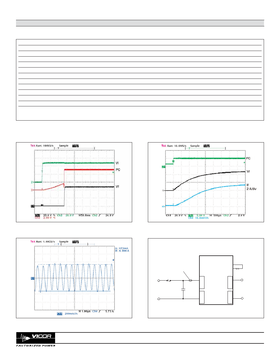
Figure 3 -- Vf turn-on waveform with inrush current ≠ PC enabled at
full load, 48 Vin
Figure 2 -- Vf and PC response from power up
Figure 4 -- Input reflected ripple current at full load and 48 Vin
Input Waveforms
+IN
≠IN
+Out
≠Out
+In
≠In
VC
PC
TM
IL
VH
PR
NC
SG
SC
PRM-AL
OS
NC
CD
100
F
Al-Electrolytic
Reflected
Ripple
Measurement
2.37 k
+ OUT
≠ OUT
10 A
Figure 5 -- Input filter capacitor recommendation
Electrical Specifications
V∑I Chip Pre-Regulator Module
vicorpower.com
800-735-6200
V∑I Chip Pre-Regulator Module
P048K048T24AL
Rev. 1.4
Page 4 of 15
PRELIMINARY
Parameter
Min
Typ
Max
Unit
Note
Output voltage range
26
48
55
Vdc
Factorized Bus voltage (Vf) set by R
OS
Output power
0
240
W
Output current
0
5
Adc
DC current limit
5.25
6.60
7.20
Adc
I
L
pin floating
Average short circuit current
0.5
A
Auto recovery
Set point accuracy
± 1.5
%
Line regulation
0.1
0.2
%
Low line to high line
Load regulation
0.1
0.2
%
No CD resistor
Load regulation (at VTM output)
1.0
%
Adaptive Loop
Current share accuracy
5
10
%
Efficiency
Full load
96
%
See Figure 7,8 & 9
Output overvoltage set point
56
59.4
Vdc
Output ripple voltage
No external bypass
1.9
2.0
%
Factorized Bus
With 10 µF capacitor
0.04
0.06
%
Factorized Bus
Switching frequency
1.35
1.45
1.55
MHz
Fixed frequency
Output turn-on delay
From application of power
150
300
ms
See Figure 2
From PC pin high
100
µs
See Figure 3
Internal output capacitance
5
µF
Ceramic
Factorized Bus capacitance
47
µF
Aluminum Electrolytic
Output Specs
(Conditions are at 48 Vin, 48 Vf, full load, and 25∞C ambient unless otherwise specified)
Output Waveforms
78
80
82
84
86
88
90
92
94
96
98
0.5
1.0
1.5
2.0
2.5
3.0
3.5
4.0
4.5
5.0
Output Current (A)
Efficiency (%)
36Vin
48Vin
75Vin
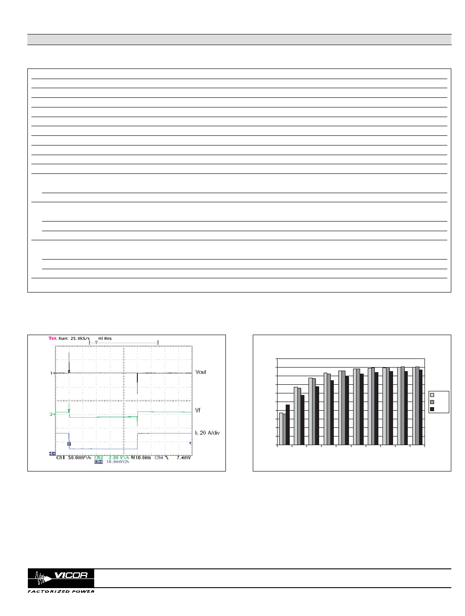
Figure 7 -- Efficiency vs. output current at 48 Vf
Figure 6 -- VTM output regulation and Vf bus during load step using
VTM with K = 1/24
Electrical Specifications
(continued)
V∑I Chip Pre-Regulator Module
vicorpower.com
800-735-6200
V∑I Chip Pre-Regulator Module
P048K048T24AL
Rev. 1.4
Page 5 of 15
PRELIMINARY
Electrical Specifications
(continued)
V∑I Chip Pre-Regulator Module
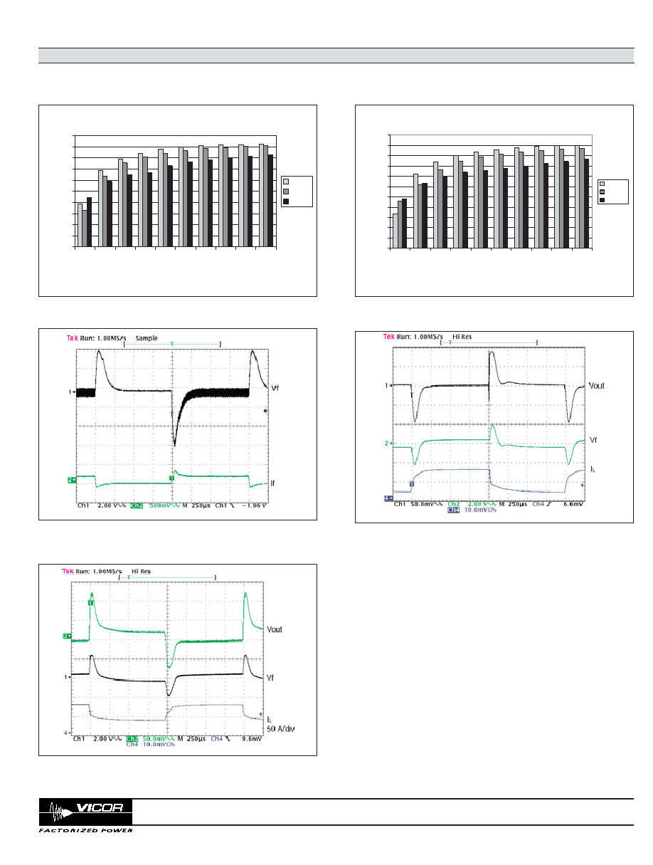
Figure 10 -- Transient response; PRM alone, 48 Vin, 0 A - 5 A, -0 A
no load capacitance. Local Loop
Figure 12 -- Transient response; load change from 40 ≠ 80 ≠ 40 A,
at the output of a K=1/24 VTM with no Vf bus capacitance and 100 µF
load capacitance.
78
80
82
84
86
88
90
92
94
96
98
0.5
1.0
1.5
2.0
2.5
3.0
3.5
4.0
4.5
5.0
Output Current (A)
Efficiency (%)
36Vin
48Vin
75Vin
Figure 8 -- Efficiency vs. output current at 36 Vf
76
78
80
82
84
86
88
90
92
94
96
98
0.5
1.0
1.5
2.0
2.5
3.0
3.5
4.0
4.5
5.0
Output Current (A)
Efficiency (%)
36Vin
48Vin
75Vin
Figure 9 -- Efficiency vs. output current at 26 Vf
Output Waveforms
Figure 11 -- Transient response; load change from 10 ≠ 40 ≠ 10 A, at
the output of a K=1/24 VTM with no Vf bus capacitance and 100 µF
load capacitance.