2N4856JAN/JANTX/JANTXV Series
Vishay Siliconix
Document Number: 70244
S-04028--Rev. C, 04-Jun-01
www.vishay.com
7-1
N-Channel JFETs
2N4856JAN
2N4856JANTX
2N4856JANTXV
2N4857JAN
2N4857JANTX
2N4857JANTXV
2N4858JAN
2N4858JANTX
2N4858JANTXV
2N4859JAN
2N4859JANTX
2N4859JANTXV
2N4860JAN
2N4860JANTX
2N4860JANTXV
2N4861JAN
2N4861JANTX
2N4861JANTXV
PRODUCT SUMMARY
Part Number
V
GS(off)
(V)
V
(BR)GSS
Min (V)
r
DS(on)
Max (
W
)
I
D(off)
Max (pA)
t
ON
Typ (ns)
2N4856
�4 to �10
�40
25
250
9
2N4857
�2 to �6
�40
40
250
10
2N4858
�0.8 to �4
�40
60
250
20
2N4859
�4 to �10
�30
25
250
9
2N4860
�2 to �6
�30
40
250
10
2N4861
�0.8 to �4
�30
60
250
20
FEATURES
BENEFITS
APPLICATIONS
D
Low On-Resistance: 2N4856 <25
W
D
Fast Switching--t
ON
: 4 ns
D
High Off-Isolation--I
D(off)
: 5 pA
D
Low Capacitance: 3 pF
D
Low Insertion Loss
D
N-Channel Majority Carrier FET
D
Low Error Voltage
D
High-Speed Analog Circuit Performance
D
Negligible "Off-Error," Excellent Accuracy
D
Good Frequency Response, Low Glitches
D
Eliminates Additional Buffering
D
High Radiation Tolerance
D
Analog Switches
D
Choppers
D
Sample-and-Hold
D
Normally "On" Switches
D
Current Limiters
DESCRIPTION
The 2N4856JAN/JANTX/JANTXV all-purpose JFET analog
switches offer low on-resistance, low capacitance, good
isolation, and fast switching.
Hermetically-sealed TO-206AA (TO-18) packaging allows full
military processing (see Military Information). For similar
products in TO-226AA (TO-92) and TO-236 (SOT-23)
packages, see the J/SST111 series data sheet. For similar
duals, see the 2N5564/5565/5566 data sheet.
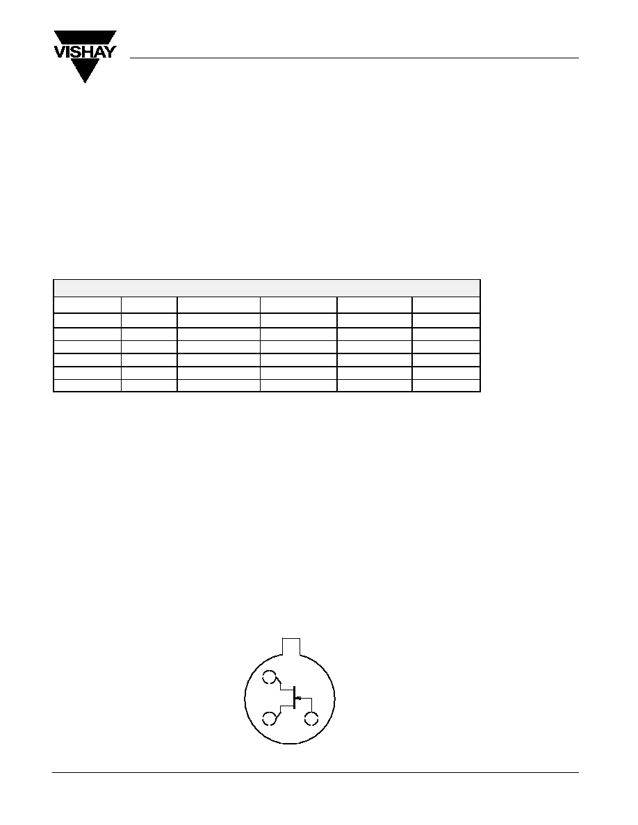
D
S
G and Case
TO-206AA
(TO-18)
Top View
1
2
3
2N4856JAN/JANTX/JANTXV Series
Vishay Siliconix
www.vishay.com
7-2
Document Number: 70244
S-04028--Rev. C, 04-Jun-01
ABSOLUTE MAXIMUM RATINGS
Gate-Drain, Gate-Source Voltage :
(2N4856-58)
�40 V
. . . . . . . . . . . . . . . . . . . . . . .
(2N4859-61)
�30 V
. . . . . . . . . . . . . . . . . . . . . . .
Gate Current
50 mA
. . . . . . . . . . . . . . . . . . . . . . . . . . . . . . . . . . . . . . . . . . . . . . . . .
Lead Temperature (
1
/
16
" from case for 10 seconds)
300
_
C
. . . . . . . . . . . . . .
Storage Temperature
�65 to 200
_
C
. . . . . . . . . . . . . . . . . . . . . . . . . . . . . . . . . . .
Operating Junction Temperature
�65 to 200
_
C
. . . . . . . . . . . . . . . . . . . . . . . . . .
Power Dissipation
a
1800 mW
. . . . . . . . . . . . . . . . . . . . . . . . . . . . . . . . . . . . . . . .
Notes
a.
Derate 10.3 mW/
_
C to T
C
> 25
_
C
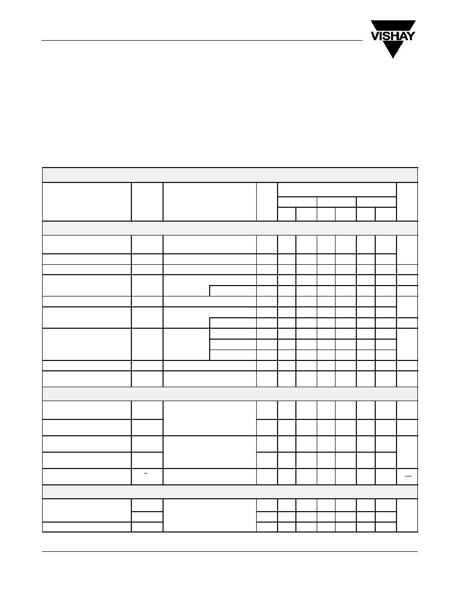
SPECIFICATIONS FOR 2N4856, 2N4857 AND 2N4858 (T
A
= 25_C UNLESS NOTED)
Limits
2N4856
2N4857
2N4858
Parameter
Symbol
Test Conditions
Typ
a
Min
Max
Min
Max
Min
Max
Unit
Static
Gate-Source
Breakdown Voltage
V
(BR)GSS
I
G
= �1
m
A , V
DS
= 0 V
�55
�40
�40
�40
V
Gate-Source Cutoff Voltage
V
GS(off)
V
DS
= 15 V, I
D
= 0.5 nA
�4
�10
�2
�6
�0.8
�4
V
Saturation Drain Current
b
I
DSS
V
DS
= 15 V, V
GS
= 0 V
50
175
20
100
8
80
mA
V
GS
= �20 V, V
DS
= 0 V
�5
�250
�250
�250
pA
Gate Reverse Current
I
GSS
T
A
= 150
_
C
�13
�500
�500
�500
nA
Gate Operating Current
c
I
G
V
DG
= 15 V, I
D
= 10 mA
�5
V
DS
= 15 V, V
GS
= �10 V
5
250
250
250
pA
Drain Cutoff Current
I
D(off)
T
A
= 150
_
C
13
500
500
500
nA
I
D
= 5 mA
0.25
0.5
Drain-Source On-Voltage
V
DS(on)
V
GS
= 0 V
I
D
= 10 mA
0.35
0.5
V
I
D
= 20 mA
0.5
0.75
Drain-Source On-Resistance
c
r
DS(on)
V
GS
= 0 V, I
D
= 1 mA
25
40
60
W
Gate-Source
Forward Voltage
c
V
GS(F)
I
G
= 1 mA , V
DS
= 0 V
0.7
V
Dynamic
Common-Source
Forward Transconductance
c
g
fs
V
DG
= 20 V, I
D
= 1 mA
6
mS
Common-Source
Output Conductance
c
g
os
V
DG
= 20 V, I
D
= 1 mA
f = 1 kHz
25
m
S
Common-Source
Input Capacitance
C
iss
V
DS
= 0 V, V
GS
= �10 V
7
18
18
18
Common-Source
Reverse Transfer Capacitance
C
rss
V
DS
= 0 V, V
GS
= �10 V
f = 1 MHz
3
8
8
8
pF
Equivalent Input
Noise Voltage
c
e
n
V
DG
= 10 V, I
D
= 10 mA
f = 1 kHz
3
nV
/
Hz
Switching
t
d(on)
2
6
6
10
Turn-On Time
t
r
V
DD
= 10 V, V
GS(H)
= 0 V
See Switching Circuit
2
3
4
10
ns
Turn-Off Time
t
OFF
See Switching Circuit
13
25
50
100
2N4856JAN/JANTX/JANTXV Series
Vishay Siliconix
Document Number: 70244
S-04028--Rev. C, 04-Jun-01
www.vishay.com
7-3
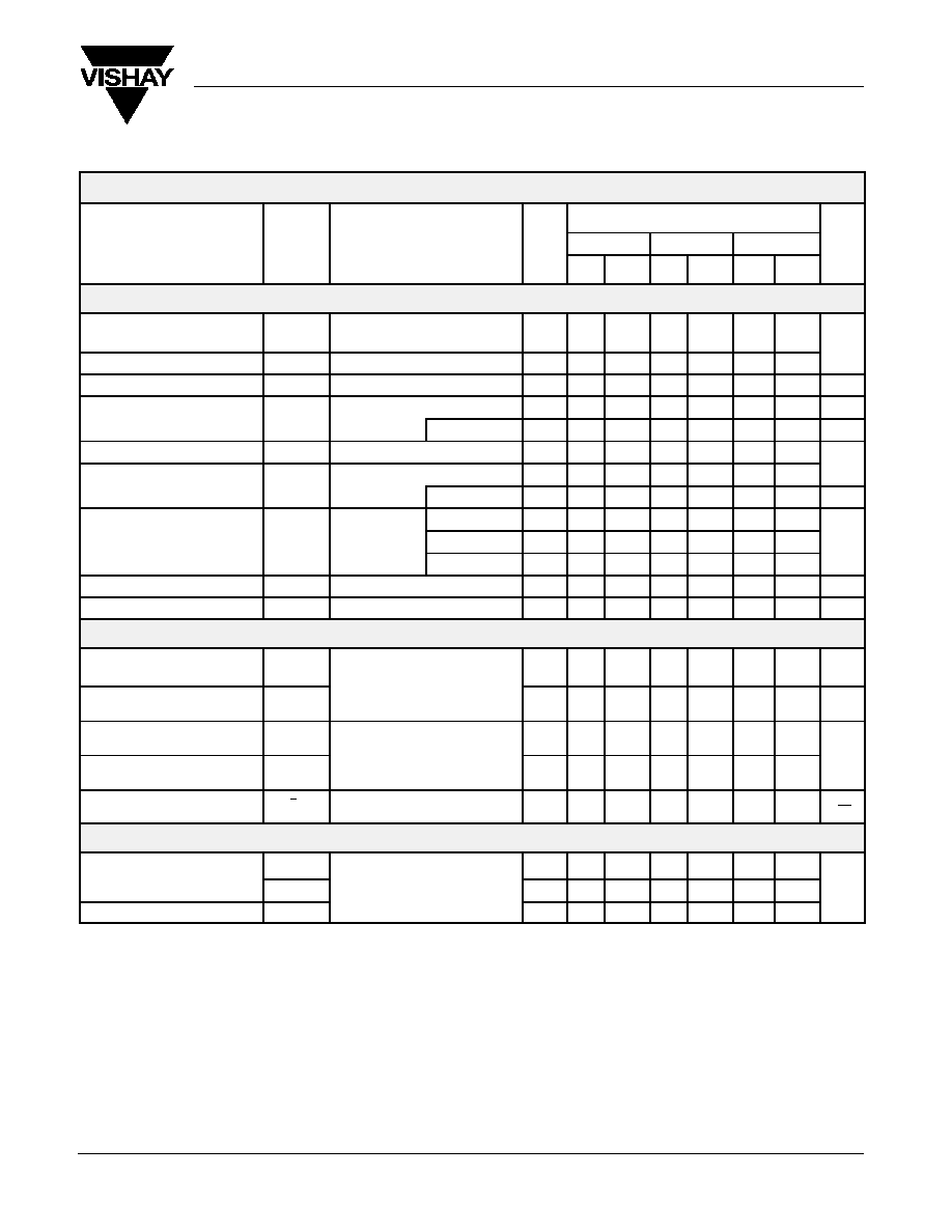
SPECIFICATIONS FOR 2N4859, 2N4860 AND 2N4861 (T
A
= 25_C UNLESS NOTED)
Limits
2N4859
2N4860
2N4861
Parameter
Symbol
Test Conditions
Typ
a
Min
Max
Min
Max
Min
Max
Unit
Static
Gate-Source
Breakdown Voltage
V
(BR)GSS
I
G
= �1
m
A , V
DS
= 0 V
�55
�30
�30
�30
V
Gate-Source Cutoff Voltage
V
GS(off)
V
DS
= 15 V, I
D
= 0.5 nA
�4
�10
�2
�6
�0.8
�4
V
Saturation Drain Current
b
I
DSS
V
DS
= 15 V, V
GS
= 0 V
50
175
20
100
8
80
mA
V
GS
= �15 V, V
DS
= 0 V
�5
�250
�250
�250
pA
Gate Reverse Current
I
GSS
T
A
= 150
_
C
�13
�500
�500
�500
nA
Gate Operating Current
c
I
G
V
DG
= 15 V, I
D
= 10 mA
�5
V
DS
= 15 V, V
GS
= �10 V
5
250
250
250
pA
Drain Cutoff Current
I
D(off)
T
A
= 150
_
C
13
500
500
500
nA
I
D
= 5 mA
0.25
0.5
Drain-Source On-Voltage
V
DS(on)
V
GS
= 0 V
I
D
= 10 mA
0.35
0.5
V
I
D
= 20 mA
0.5
0.75
Drain-Source On-Resistance
r
DS(on)
V
GS
= 0 V, I
D
= 1 mA
25
40
60
W
Gate-Source Forward Voltage
V
GS(F)
I
G
= 1 mA , V
DS
= 0 V
0.7
V
Dynamic
Common-Source
Forward Transconductance
c
g
fs
V
DG
= 20 V, I
D
= 1 mA
6
mS
Common-Source
Output Conductance
c
g
os
V
DG
= 20 V, I
D
= 1 mA
f = 1 kHz
25
m
S
Common-Source
Input Capacitance
C
iss
V
DS
= 0 V, V
GS
= �10 V
7
18
18
18
Common-Source
Reverse Transfer Capacitance
C
rss
V
DS
= 0 V, V
GS
= �10 V
f = 1 MHz
3
8
8
8
pF
Equivalent Input
Noise Voltage
c
e
n
V
DG
= 10 V, I
D
= 10 mA
f = 1 kHz
3
nV
/
Hz
Switching
t
d(on)
2
6
6
10
Turn-On Time
t
r
V
DD
= 10 V, V
GS(H)
= 0 V
See Switching Circuit
2
3
4
10
ns
Turn-Off Time
t
OFF
See Switching Circuit
19
25
50
100
Notes
a.
Typical values are for DESIGN AID ONLY, not guaranteed nor subject to production testing.
NCB
b.
Pulse test: PW
v
100
m
s duty cycle
v
10%.
c.
This parameter not registered with JEDEC.
2N4856JAN/JANTX/JANTXV Series
Vishay Siliconix
www.vishay.com
7-4
Document Number: 70244
S-04028--Rev. C, 04-Jun-01
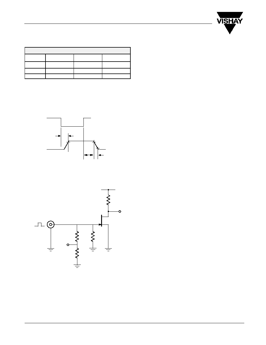
SWITCHING TIME TEST CIRCUIT
4856/4859
4857/4860
4858/4861
V
GS(L)
�10 V
�6 V
�4 V
R
L
*
464
W
953
W
1910
W
I
D(on)
20 mA
10 mA
5 mA
*Non-inductive
INPUT PULSE
SAMPLING SCOPE
Rise Time < 1 ns
Fall Time < 1 ns
Pulse Width 100 ns
PRF 1 MHz
Rise Time 0.4 ns
Input Resistance 10 M
W
Input Capacitance 1.5 pF
51
51
1 k
V
IN
Scope
V
DD
R
L
OUT
t
OFF
OUTPUT
t
r
<20 ns
t
f
<20 ns
10%
90%
V
IN
INPUT
t
r
t
d(on)
V
GS(H)
V
GS(L)