 | –≠–ª–µ–∫—Ç—Ä–æ–Ω–Ω—ã–π –∫–æ–º–ø–æ–Ω–µ–Ω—Ç: 83143 | –°–∫–∞—á–∞—Ç—å:  PDF PDF  ZIP ZIP |
VISHAY
TLMW310.
Document Number 83143
Rev. 1.7, 31-Aug-04
Vishay Semiconductors
www.vishay.com
1
e3 Pb
Pb-free
19225
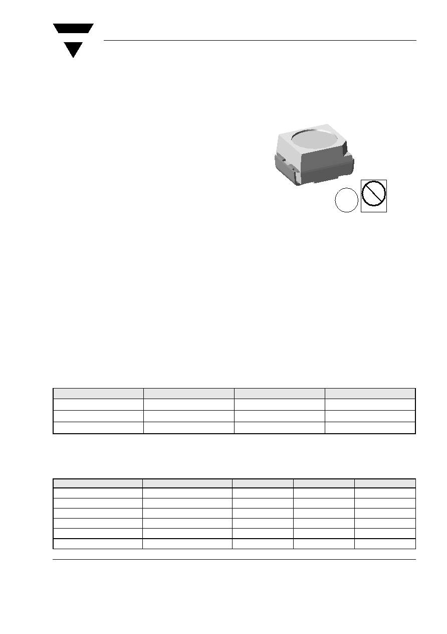
High Intensity SMD LED
Description
This device has been designed to meet the increasing
demand for white SMD LED.
The package of the TLMW310. is the PLCC-2 (equiv-
alent to a size B tantalum capacitor).
It consists of a lead frame which is embedded in a
white thermoplast. The reflector inside this package is
filled with a mixture of epoxy and TAG phosphor.
The TAG phosphor converts the blue emission par-
tially to yellow, which mixes with the remaining blue to
give white.
Features
∑ High efficient InGaN technology
∑ Chromaticity Coordinate categorized according to
CIE1931 per packing unit
∑ Luminous intensity ratio in one packing unit
I
Vmax
/I
Vmin
1.6
∑ Typical color temperature 5500 K
∑ ESD class 1
∑ EIA and ICE standard package
∑ Compatible with infrared, vapor phase and wave
solder processes according to CECC
∑ Available in 8 mm tape reel
∑ Lead-free device
Applications
Automotive: Backlighting in dashboards and switches
Telecommunication: Indicator and backlighting in
telephone and fax
Backlighting for audio and video equipment
Backlighting in office equipment
Indoor and outdoor message boards
Flat backlight for LCDs, switches and symbols
Illumination purposes, alternative to incandescent
lamps
General use
Parts Table
Absolute Maximum Ratings
T
amb
= 25 ∞C, unless otherwise specified
TLMW310.
Part
Color, Luminous Intensity
Angle of Half Intensity (±
)
Technology
TLMW3100
White, I
V
> 80 mcd
60 ∞
InGaN / TAG on SiC
TLMW3101
White, I
V
= (80 to 200) mcd
60 ∞
InGaN / TAG on SiC
TLMW3102
White, I
V
= (125 to 320) mcd
60 ∞
InGaN / TAG on SiC
Parameter
Test condition
Symbol
Value
Unit
Reverse voltage
V
R
5
V
DC Forward current
T
amb
70 ∞C
I
F
20
mA
Surge forward current
t
p
10 µs
I
FSM
0.1
A
Power dissipation
T
amb
70 ∞C
P
V
85
mW
Junction temperature
T
j
100
∞C
Operating temperature range
T
amb
- 40 to + 100
∞C
www.vishay.com
2
Document Number 83143
Rev. 1.7, 31-Aug-04
VISHAY
TLMW310.
Vishay Semiconductors
Optical and Electrical Characteristics
T
amb
= 25 ∞C, unless otherwise specified
White
TLMW310.
1)
in one Packing Unit I
Vmax
/I
Vmin
1.6
Typical Characteristics
(T
amb
= 25
∞C unless otherwise specified)
Storage temperature range
T
stg
- 40 to + 100
∞C
Soldering temperature
t
5 s
T
sd
260
∞C
Thermal resistance junction/
ambient
mounted on PC board
(pad size > 16 mm
2
)
R
thJA
350
K/W
Parameter
Test condition
Part
Symbol
Min
Typ.
Max
Unit
Luminous intensity
1)
I
F
= 20 mA
TLMW3100
I
V
80
140
mcd
TLMW3101
I
V
80
200
mcd
TLMW3102
I
V
125
320
mcd
Chromaticity coordinate x acc.
to CIE 1931
I
F
= 20 mA
TLMW3100
x
0.33
Chromaticity coordinate y acc.
to CIE 1931
I
F
= 20 mA
TLMW3100
y
0.33
Angle of half intensity
I
F
= 20 mA
± 60
deg
Forward voltage
I
F
= 20 mA
V
F
3.5
4.2
V
Reverse voltage
I
R
= 10
µA
V
R
5
V
Temperature coefficient of V
F
I
F
= 20 mA
TC
VF
- 4
mV/K
Temperature coefficient of I
V
I
F
= 20 mA
TC
IV
- 0.5
% / K
Parameter
Test condition
Symbol
Value
Unit
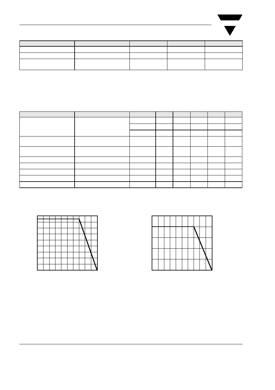
Figure 1. Power Dissipation vs. Ambient Temperature
P
-
Power
Dissipation
(
m
W
)
V
0
10
20
30
40
50
60
70
80
90
T
amb
- Ambient Temperature (
∞C )
16191
0
10 20
30 40 50 60 70 80 90 100
Figure 2. Forward Current vs. Ambient Temperature for AlInGaP
0
5
10
15
20
25
16192
I
-
Forward
Current
(
m
A
)
F
T
amb
- Ambient Temperature ( ∞ C )
0 10 20 30 40 50 60 70 80 90 100

VISHAY
TLMW310.
Document Number 83143
Rev. 1.7, 31-Aug-04
Vishay Semiconductors
www.vishay.com
3
Figure 3. Forward Current vs. Ambient Temperature for AlInGaP
Figure 4. Relative Luminous Intensity vs. Forward Current
Figure 5. Forward Current vs. Forward Voltage
0
5
10
15
20
25
30
0
10 20 30 40 50 60 70 80 90 100
T
amb
- Ambient Temperature (
∞C )
16193
I
-
Forward
Current
(
m
A
)
F
MTTF, confidence level 60%
failure criteria I
V
/I
V0
= 50%
II
I
I
i
5000h
II
i 10000h
0.01
0.1
1
10
1
10
100
I
F
- Forward Current ( mA )
16194
I
-
Relative
Luminous
Intensity
Vrel
1
10
100
2.0
2.5
3.0
3.5
4.0
4.5
5.0
V
F
- Forward Voltage ( V )
16195
F
I
-
Forward
Current
(
m
A
)
Figure 6. Relative Intensity vs. Wavelength
Figure 7. Rel. Luminous Intensity vs. Ambient Temperature
Figure 8. Chromaticity Coordinate Shift vs. Forward Current
0
10
20
30
40
50
60
70
80
90
100
400 450 500 550 600 650 700 750 800
- Wavelength ( nm )
16196
I
-
Relative
Luminous
Intensity
V
rel
0.0
0.2
0.4
0.6
0.8
1.0
1.2
1.4
1.6
1.8
2.0
16197
I
-
Relative
Luminous
Intensity
Vrel
T
amb
- Ambient Temperature ( ∞C )
0 10 20 30 40 50 60 70 80 90 100
0.315
0.320
0.325
0.330
0.335
0.340
0.345
16198
f
-
Chromaticity
coordinate
shift
(x,y)
X
Y
I
F
- Forward Current ( mA )
White
0
60
50
40
30
20
10

www.vishay.com
4
Document Number 83143
Rev. 1.7, 31-Aug-04
VISHAY
TLMW310.
Vishay Semiconductors
Figure 9. Forward Voltage vs. Ambient Temperature
Figure 10. Rel. Luminous Intensity vs. Angular Displacement
Figure 11. Coordinates of Colorgroups
3.45
3.50
3.55
3.60
3.65
3.70
3.75
3.80
3.85
3.90
3.95
16199
I
-
Forward
Voltag
e(V)
F
T
amb
- Ambient Temperature (
∞C )
0 10 20
30 40 50 60 70 80 90 100
0.4
0.2
0
0.2
0.4
0.6
95 10319
0.6
0.9
0.8
0∞
30∞
10∞
20∞
40∞
50∞
60∞
70∞
80∞
0.7
1.0
I
-
Relative
Luminous
Intensity
Vr
e
l
0.20
0.25
0.30
0.35
0.40
0.45
0.50
0.20
0.25
0.30
0.35
0.40
0.45
0.50
16284
Coordinates of Colorgroups
a = 20000K
b = 10000K
c = 7000K
d = 6000K
e = 5000K
f =
4000K
a
b
c
d
e
f
3
4
5
.
.
A
D65
Coordinates
of
Colorgroups
VISHAY
TLMW310.
Document Number 83143
Rev. 1.7, 31-Aug-04
Vishay Semiconductors
www.vishay.com
5
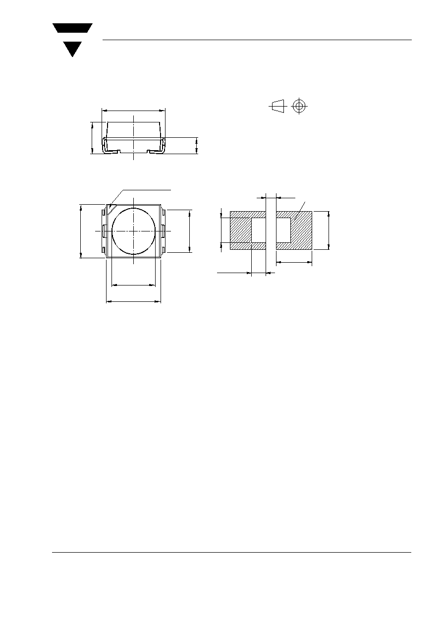
Package Dimensions in mm
95 11314
Mounting Pad Layout
3.5 ± 0.2
0.85
1.65
+
0.10
-
0.05
Pin identification
2.8
+
0.15
2.2
2.4
3
+ 0.15
1.2
2.6
(2.8)
1.6 (1.9)
4
4
area covered with
solder resist
Dimensions: IR and Vaporphase
(Wave Soldering)
technical drawings
according to DIN
specifications
Drawing-No. : 6.541-5025.01-4
Issue: 7; 05.04.04
C
A

www.vishay.com
6
Document Number 83143
Rev. 1.7, 31-Aug-04
VISHAY
TLMW310.
Vishay Semiconductors
Ozone Depleting Substances Policy Statement
It is the policy of Vishay Semiconductor GmbH to
1. Meet all present and future national and international statutory requirements.
2. Regularly and continuously improve the performance of our products, processes, distribution and
operatingsystems with respect to their impact on the health and safety of our employees and the public, as
well as their impact on the environment.
It is particular concern to control or eliminate releases of those substances into the atmosphere which are
known as ozone depleting substances (ODSs).
The Montreal Protocol (1987) and its London Amendments (1990) intend to severely restrict the use of ODSs
and forbid their use within the next ten years. Various national and international initiatives are pressing for an
earlier ban on these substances.
Vishay Semiconductor GmbH has been able to use its policy of continuous improvements to eliminate the
use of ODSs listed in the following documents.
1. Annex A, B and list of transitional substances of the Montreal Protocol and the London Amendments
respectively
2. Class I and II ozone depleting substances in the Clean Air Act Amendments of 1990 by the Environmental
Protection Agency (EPA) in the USA
3. Council Decision 88/540/EEC and 91/690/EEC Annex A, B and C (transitional substances) respectively.
Vishay Semiconductor GmbH can certify that our semiconductors are not manufactured with ozone depleting
substances and do not contain such substances.
We reserve the right to make changes to improve technical design
and may do so without further notice.
Parameters can vary in different applications. All operating parameters must be validated for each
customer application by the customer. Should the buyer use Vishay Semiconductors products for any
unintended or unauthorized application, the buyer shall indemnify Vishay Semiconductors against all
claims, costs, damages, and expenses, arising out of, directly or indirectly, any claim of personal
damage, injury or death associated with such unintended or unauthorized use.
Vishay Semiconductor GmbH, P.O.B. 3535, D-74025 Heilbronn, Germany
Telephone: 49 (0)7131 67 2831, Fax number: 49 (0)7131 67 2423