BA1282.BA1283
Vishay Telefunken
Rev. 2, 01-Apr-99
1 (4)
www.vishay.de
∑
FaxBack +1-408-970-5600
Document Number 85525
Silicon Planar Diodes
Features
D
Saving space
D
Hermetic sealed parts
D
Fits onto SOD 323 footprints
D
Electrical data identical with the devices
BA682.BA683 / BA982.BA983
D
Low differential forward resistance
D
Low diode capacitance
D
High reverse impedance
Applications
Band switching in VHF≠tuners
96 12315
Absolute Maximum Ratings
T
j
= 25
_
C
Parameter
Test Conditions
Type
Symbol
Value
Unit
Reverse voltage
V
R
35
V
Forward current
I
F
100
mA
Junction temperature
T
j
150
∞
C
Storage temperature range
T
stg
≠55...+150
∞
C
Maximum Thermal Resistance
T
j
= 25
_
C
Parameter
Test Conditions
Symbol
Value
Unit
Junction ambient
mounted on epoxy≠glass hard tissue,
Fig. 1 35
m
m copper clad, 0.9 mm
2
copper
area per electrode
R
thJA
500
K/W
BA1282.BA1283
Vishay Telefunken
Rev. 2, 01-Apr-99
2 (4)
www.vishay.de
∑
FaxBack +1-408-970-5600
Document Number 85525
Electrical Characteristics
T
j
= 25
_
C
Parameter
Test Conditions
Type
Symbol
Min
Typ
Max
Unit
Forward voltage
I
F
=100mA
V
F
1
V
Reverse current
V
R
=20V
I
R
50
nA
Diode capacitance
f=100MHz, V
R
=1V
C
D
1.5
pF
f=100MHz, V
R
=3V
BA1282
C
D
1.25
pF
f=100MHz, V
R
=3V
BA1283
C
D
1.2
pF
Differential forward
f=200MHz, I
F
=3mA
BA1282
r
f
0.7
W
resistance
f=200MHz, I
F
=3mA
BA1283
r
f
1.2
W
f=200MHz, I
F
=10mA
BA1282
r
f
0.5
W
f=200MHz, I
F
=10mA
BA1283
r
f
0.9
W
Characteristics (T
j
= 25
_
C unless otherwise specified)
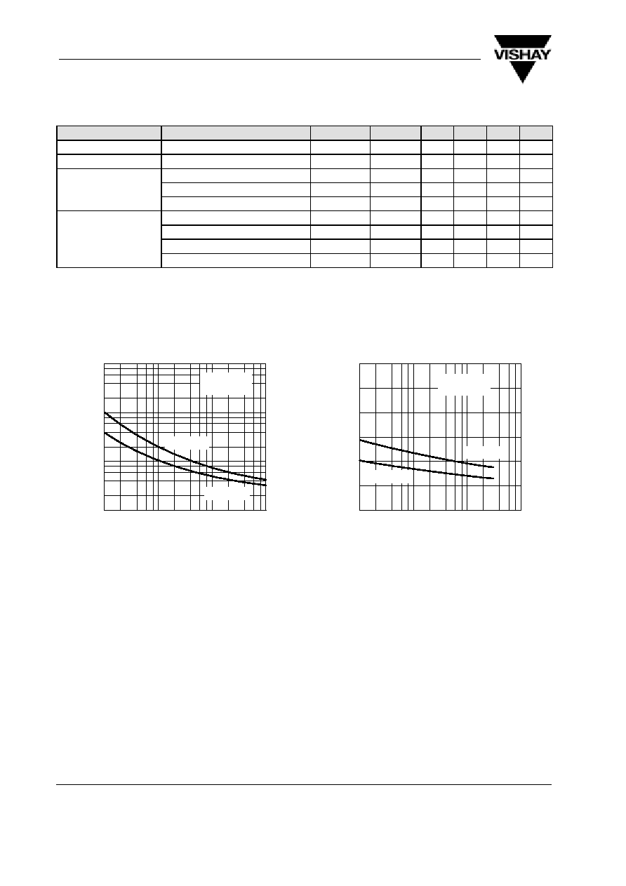
0.1
1
10
0.1
1
10
100
r ≠ Dif
ferential Forward Resistance ( )
f
I
F
≠ Forward Current ( mA )
100
94 9076
W
BA1282
BA 1283
f = 200 MHz
T
j
= 25
∞
C
Figure 1. Differential Forward Resistance vs.
Forward Current
0.1
1
10
0
0.5
1.0
1.5
2.0
3.0
C ≠ Diode Capacitance ( pF )
D
V
R
≠ Reverse Voltage ( V )
100
94 9077
2.5
BA1282
BA1283
f = 100 MHz
T
j
= 25
∞
C
Figure 2. Diode Capacitance vs. Reverse Voltage

BA1282.BA1283
Vishay Telefunken
Rev. 2, 01-Apr-99
4 (4)
www.vishay.de
∑
FaxBack +1-408-970-5600
Document Number 85525
Ozone Depleting Substances Policy Statement
It is the policy of Vishay Semiconductor GmbH to
1. Meet all present and future national and international statutory requirements.
2. Regularly and continuously improve the performance of our products, processes, distribution and operating
systems
with respect to their impact on the health and safety of our employees and the public, as well as their impact on
the environment.
It is particular concern to control or eliminate releases of those substances into the atmosphere which are known
as ozone depleting substances ( ODSs ).
The Montreal Protocol ( 1987 ) and its London Amendments ( 1990 ) intend to severely restrict the use of ODSs and
forbid their use within the next ten years. Various national and international initiatives are pressing for an earlier ban
on these substances.
Vishay Semiconductor GmbH has been able to use its policy of continuous improvements to eliminate the use
of ODSs listed in the following documents.
1. Annex A, B and list of transitional substances of the Montreal Protocol and the London Amendments respectively
2 . Class I and II ozone depleting substances in the Clean Air Act Amendments of 1990 by the Environmental
Protection Agency ( EPA ) in the USA
3. Council Decision 88/540/EEC and 91/690/EEC Annex A, B and C ( transitional substances ) respectively.
Vishay Semiconductor GmbH can certify that our semiconductors are not manufactured with ozone depleting
substances and do not contain such substances.
We reserve the right to make changes to improve technical design and may do so without further notice.
Parameters can vary in different applications. All operating parameters must be validated for each customer
application by the customer. Should the buyer use Vishay-Telefunken products for any unintended or unauthorized
application, the buyer shall indemnify Vishay-Telefunken against all claims, costs, damages, and expenses, arising out
of, directly or indirectly, any claim of personal damage, injury or death associated with such unintended or
unauthorized use.
Vishay Semiconductor GmbH, P.O.B. 3535, D-74025 Heilbronn, Germany
Telephone: 49 ( 0 ) 7131 67 2831, Fax number: 49 ( 0 ) 7131 67 2423