VISHAY
BA892V-02V
Document Number 85640
Rev. 1, 26-Sep-02
Vishay Semiconductors
www.vishay.com
1
16863
C
A
Band Switching Diodes
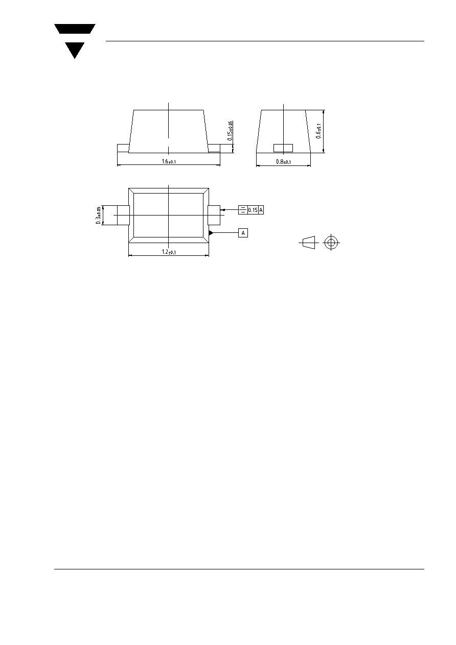
Mechanical Data
Case: Plastic case (SOD 523)
Weight: 1.5 mg
Cathode Band Color: Laser marking
Packaging Codes/Options:
GS08 / 3 k per 7" reel (8 mm tape), 3 k/Box
Description
The main purpose of the BA892V-02V is the Band
Switching. Biased with a DC forward current for sig-
nals at frequencies over 100 MHz up to 3 GHz this di-
ode behaves like a current controlled resistor and not
as a diode any more.
Depending on the forward current the forward resis-
tance rf can be switched far below 1
, so that the
Switch is closed. To open the Switch, the BA892V-
02V has to be driven in the reverse mode where the
BA892V-02V behaves like a small capacitor with high
isolation. So typical applications for this Band Switch-
ing Diode are mobile and TV-applications.
Features
� Low forward resistance
� Small, space saving SOD523 package with low
series inductance
� Small capacitance
Applications
� Band switching up to 3 GHz
� Low loss band-switching in TV/VTR tuners
Parts Table
Absolute Maximum Ratings
T
amb
= 25 �C, unless otherwise specified
Maximum Thermal Resistance
T
amb
= 25 �C, unless otherwise specified
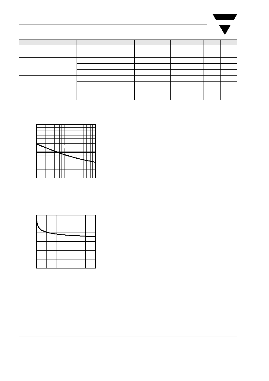
Electrical Characteristics
T
amb
= 25 �C, unless otherwise specified
Part
Ordering code
Marking
Remarks
Package
BA892V-02V
BA892V-02V-GS08
A
Tape and Reel
SOD523
Parameter
Test condition
Sub type
Symbol
Value
Unit
Reverse voltage
V
R
35
V
Forward current
I
F
100
mA
Junction temperature
T
j
150
�C
Storage temperature range
T
stg
-55 to
+150
�C
Parameter
Test condition
Symbol
Value
Unit
Junction soldering point
R
thJS
100
K/W
Parameter
Test condition
Sub type
Symbol
Min
Typ.
Max
Unit
Reverse voltage
I
R
= 10 �A
V
R
35
V

Document Number 85640
Rev. 1, 26-Sep-02
www.vishay.com
4
VISHAY
BA892V-02V
Vishay Semiconductors
Ozone Depleting Substances Policy Statement
It is the policy of Vishay Semiconductor GmbH to
1. Meet all present and future national and international statutory requirements.
2. Regularly and continuously improve the performance of our products, processes, distribution and
operatingsystems with respect to their impact on the health and safety of our employees and the public, as
well as their impact on the environment.
It is particular concern to control or eliminate releases of those substances into the atmosphere which are
known as ozone depleting substances (ODSs).
The Montreal Protocol (1987) and its London Amendments (1990) intend to severely restrict the use of ODSs
and forbid their use within the next ten years. Various national and international initiatives are pressing for an
earlier ban on these substances.
Vishay Semiconductor GmbH has been able to use its policy of continuous improvements to eliminate the
use of ODSs listed in the following documents.
1. Annex A, B and list of transitional substances of the Montreal Protocol and the London Amendments
respectively
2. Class I and II ozone depleting substances in the Clean Air Act Amendments of 1990 by the Environmental
Protection Agency (EPA) in the USA
3. Council Decision 88/540/EEC and 91/690/EEC Annex A, B and C (transitional substances) respectively.
Vishay Semiconductor GmbH can certify that our semiconductors are not manufactured with ozone depleting
substances and do not contain such substances.
We reserve the right to make changes to improve technical design and may do so without further
notice.
Parameters can vary in different applications. All operating parameters must be validated for each
customer application by the customer. Should the buyer use Vishay Semiconductors products for any
unintended or unauthorized application, the buyer shall indemnify Vishay Seminconductors against all
claims, costs, damages, and expenses, arising out of, directly or indirectly, any claim of personal
damage, injury or death associated with such unintended or unauthorized use.
Vishay Semiconductor GmbH, P.O.B. 3535, D-74025 Heilbronn, Germany
Telephone: 49 (0)7131 67 2831, Fax number: 49 (0)7131 67 2423