 | ÐлекÑÑоннÑй компоненÑ: BAS386-TR | СкаÑаÑÑ:  PDF PDF  ZIP ZIP |
Äîêóìåíòàöèÿ è îïèñàíèÿ www.docs.chipfind.ru
BAS386
Document Number 85505
Rev. 1.9, 07-Mar-06
Vishay Semiconductors
www.vishay.com
1
9612315
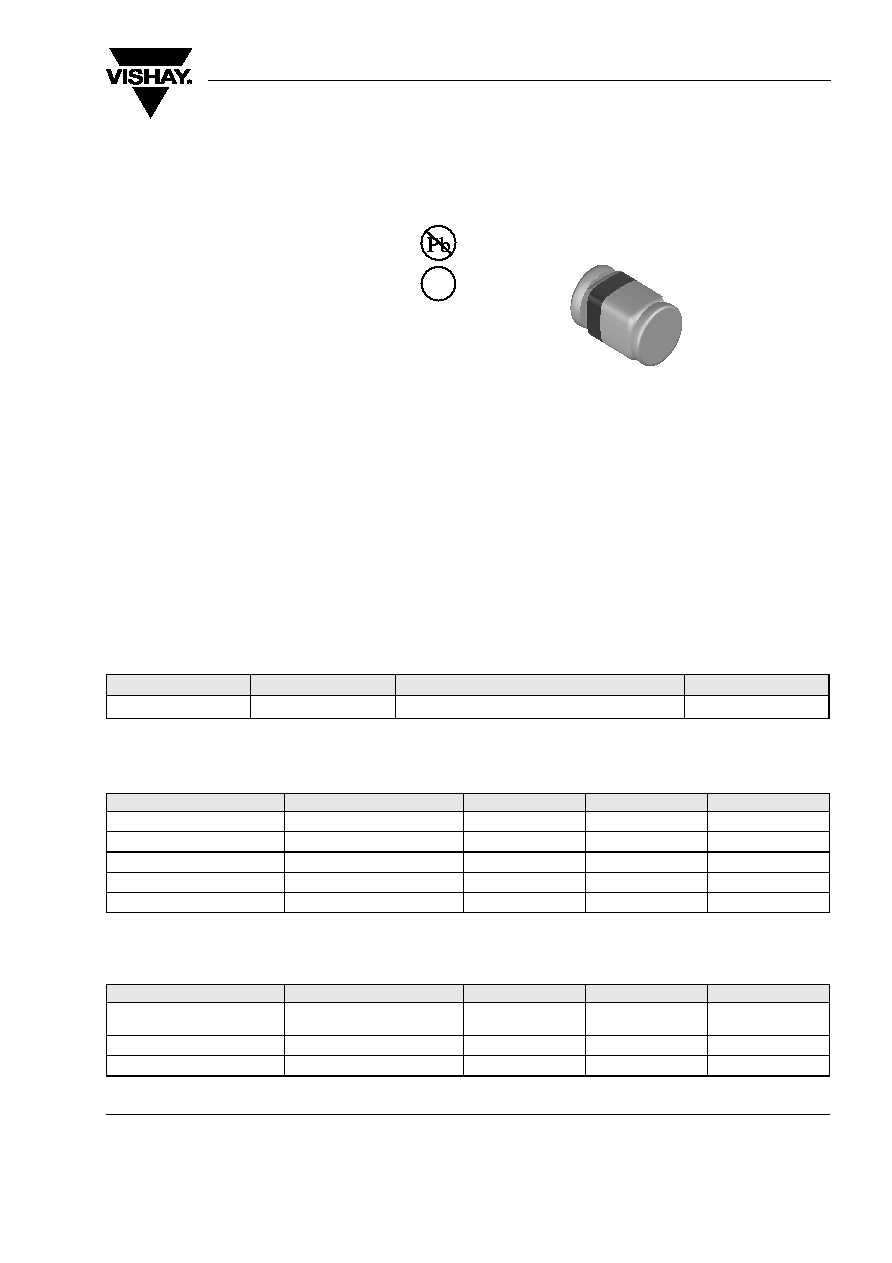
Small Signal Schottky Diode
Features
· Integrated protection ring against static
discharge
· Very low forward voltage
· Lead (Pb)-free component
· Component in accordance to RoHS 2002/95/EC
and WEEE 2002/96/EC
Applications
· Applications where a very low forward voltage is
required
Mechanical Data
Case: MicroMELF Glass case
Weight: approx. 12 mg
Cathode Band Color: Black
Packaging Codes/Options:
TR3 / 10 k per 13" reel (8 mm tape), 10 k/box
TR / 2.5 k per 7" reel (8 mm tape), 12.5 k/box
Parts Table
Absolute Maximum Ratings
T
amb
= 25 °C, unless otherwise specified
Thermal Characteristics
T
amb
= 25 °C, unless otherwise specified
Part
Type differentiation
Ordering code
Remarks
BAS386
V
R
= 50 V
BAS386-TR3 or BAS386-TR
Tape and Reel
Parameter
Test condition
Symbol
Value
Unit
Reverse voltage
V
R
50
V
Peak forward surge current
t
p
= 10 ms
I
FSM
5
A
Repetitive peak forward current
t
p
1 s
I
FRM
500
mA
Forward continuous current
I
F
200
mA
Average forward current
I
FAV
200
mA
Parameter
Test condition
Symbol
Value
Unit
Junction to ambient air
on PC board
50 mm x 50 mm x 1.6 mm
R
thJA
320
K/W
Junction temperature
T
j
125
°C
Storage temperature range
T
stg
- 65 to + 150
°C
e2
www.vishay.com
2
Document Number 85505
Rev. 1.9, 07-Mar-06
BAS386
Vishay Semiconductors
Electrical Characteristics
T
amb
= 25 °C, unless otherwise specified
Typical Characteristics
T
amb
= 25 °C, unless otherwise specified
Parameter
Test condition
Symbol
Min
Typ.
Max
Unit
Forward voltage
I
F
= 0.1 mA
V
F
300
mV
I
F
= 1 mA
V
F
380
mV
I
F
= 10 mA
V
F
450
mV
I
F
= 30 mA
V
F
600
mV
I
F
= 100 mA
V
F
900
mV
Reverse current
V
R
= 40 V
I
R
5
µA
Diode capacitance
V
R
= 1 V, f = 1 MHz
C
D
8
pF
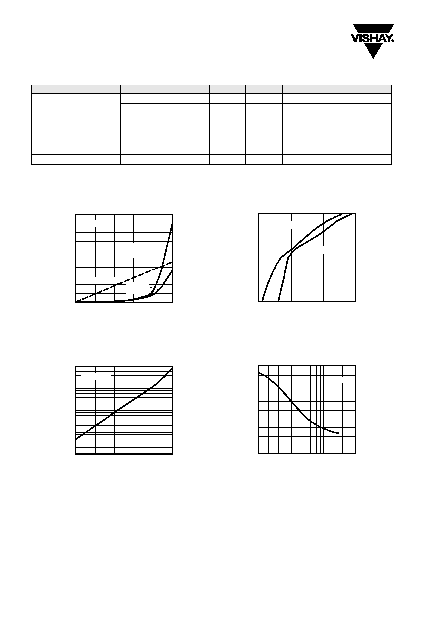
Figure 1. Max. Reverse Power Dissipation vs. Junction
Temperature
Figure 2. Reverse Current vs. Junction Temperature
15827
0
50
100
150
200
250
300
350
400
450
500
25
50
75
100
125
150
T
j
- Junction Temperature (°C)
P-
R
e
v
erse
Po
w
er
Dissipation (m
W
)
R
- Limit
at 100 % V
P
R
R
- Limit
at 80 % V
P
R
R
R
thJA
= 540 K/W
V
R
= 50 V
1
10
100
1000
10000
25
50
75
100
125
150
15828
I-
R
e
v
erse
C
u
rrent (
µ
A)
R
T
j
- Junction Temperature (°C)
V
R
= V
RRM
Figure 3. Forward Current vs. Forward Voltage
Figure 4. Diode Capacitance vs. Reverse Voltage
15829
0
0.5
1.0
1.5
0.1
1
10
100
1000
I
-
For
w
ard
C
u
rrent (A)
F
V
F
- Forward Voltage (V)
T
j
= 25 °C
T
j
= 150 °C
15830
0
1
2
3
4
5
6
7
8
9
10
0.1
1
10
100
f = 1 MHz
V
R
- Reverse Voltage (V)
C
-
Diode
Capacitance (pF)
D
BAS386
Document Number 85505
Rev. 1.9, 07-Mar-06
Vishay Semiconductors
www.vishay.com
3
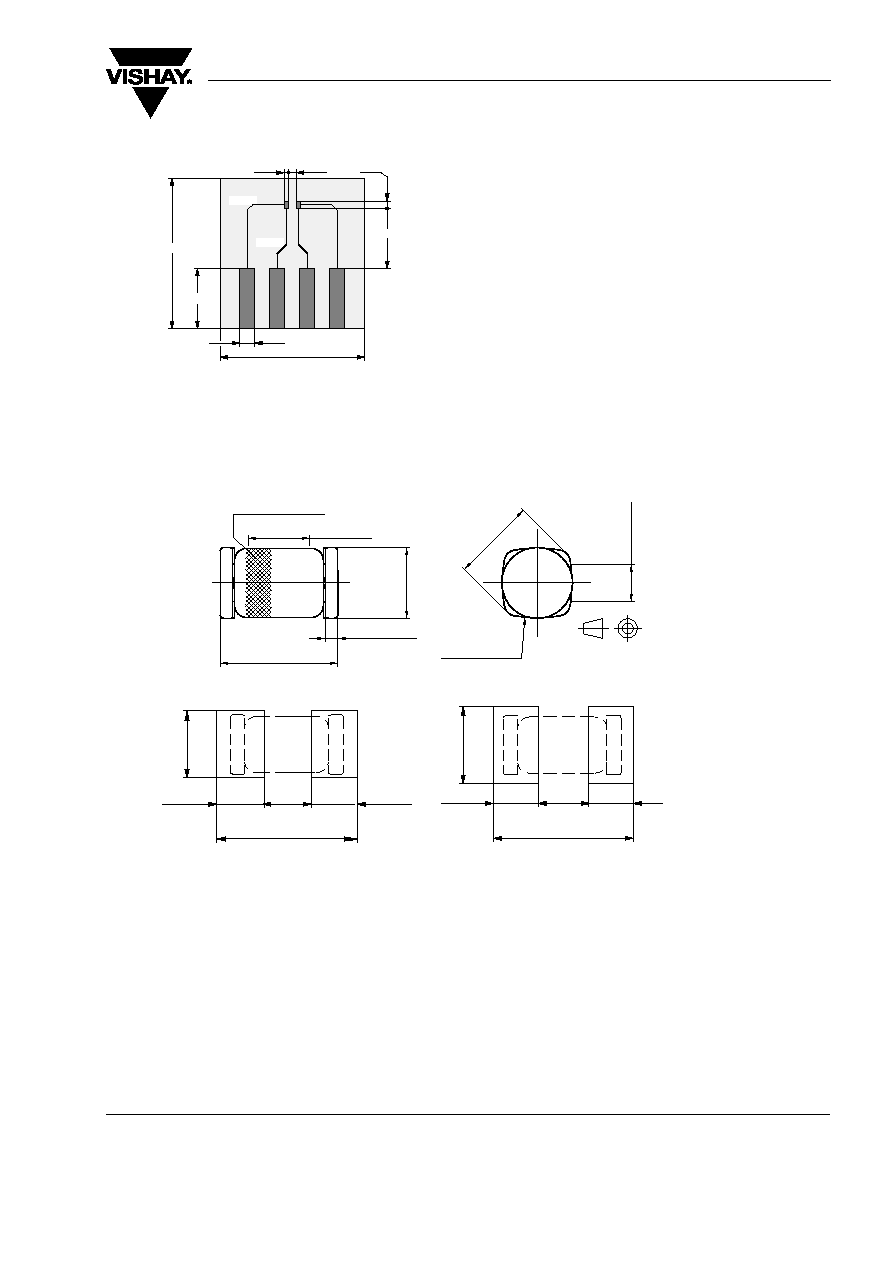
Package Dimensions in mm (Inches)
Figure 5. Board for R
thJA
definition (in mm)
25
2.5
10
0.71
1.3
1.27
9.9
24
0.152
0.355
95 10329
ISO Method E
9612072
2.8 (0.110)
0.9 (0.035)
0.9 (0.035)
Reflow Soldering
Wave Soldering
1.0 (0.039)
1.4
(0.055)
Cathode indification
1 (0.039) surface plan
2.0 (0.079)
1.8 (0.071)
0.25 (0.010)
0.15 (0.006)
1.2
(0.047)
1.1
(0.043)
Glass case
MicroMELF
Glass
<
1.35
(0.053
)
> R 2.5 (R 0.098)
Glass
0.6
(0.024)
s
u
rface
plan
Document No.: 6.560-5007.01-4
Rev. 11, 07.Feb.2005
1.2 (0.047)
2.4 (0.094)
0.8 (0.031)
0.8 (0.031)
0.8 (0.031)

www.vishay.com
4
Document Number 85505
Rev. 1.9, 07-Mar-06
BAS386
Vishay Semiconductors
Ozone Depleting Substances Policy Statement
It is the policy of Vishay Semiconductor GmbH to
1. Meet all present and future national and international statutory requirements.
2. Regularly and continuously improve the performance of our products, processes, distribution and operating
systems with respect to their impact on the health and safety of our employees and the public, as well as
their impact on the environment.
It is particular concern to control or eliminate releases of those substances into the atmosphere which are
known as ozone depleting substances (ODSs).
The Montreal Protocol (1987) and its London Amendments (1990) intend to severely restrict the use of ODSs
and forbid their use within the next ten years. Various national and international initiatives are pressing for an
earlier ban on these substances.
Vishay Semiconductor GmbH has been able to use its policy of continuous improvements to eliminate the use
of ODSs listed in the following documents.
1. Annex A, B and list of transitional substances of the Montreal Protocol and the London Amendments
respectively
2. Class I and II ozone depleting substances in the Clean Air Act Amendments of 1990 by the Environmental
Protection Agency (EPA) in the USA
3. Council Decision 88/540/EEC and 91/690/EEC Annex A, B and C (transitional substances) respectively.
Vishay Semiconductor GmbH can certify that our semiconductors are not manufactured with ozone depleting
substances and do not contain such substances.
We reserve the right to make changes to improve technical design
and may do so without further notice.
Parameters can vary in different applications. All operating parameters must be validated for each
customer application by the customer. Should the buyer use Vishay Semiconductors products for any
unintended or unauthorized application, the buyer shall indemnify Vishay Semiconductors against all
claims, costs, damages, and expenses, arising out of, directly or indirectly, any claim of personal
damage, injury or death associated with such unintended or unauthorized use.
Vishay Semiconductor GmbH, P.O.B. 3535, D-74025 Heilbronn, Germany

Legal Disclaimer Notice
Vishay
Document Number: 91000
www.vishay.com
Revision: 08-Apr-05
1
Notice
Specifications of the products displayed herein are subject to change without notice. Vishay Intertechnology, Inc.,
or anyone on its behalf, assumes no responsibility or liability for any errors or inaccuracies.
Information contained herein is intended to provide a product description only. No license, express or implied, by
estoppel or otherwise, to any intellectual property rights is granted by this document. Except as provided in Vishay's
terms and conditions of sale for such products, Vishay assumes no liability whatsoever, and disclaims any express
or implied warranty, relating to sale and/or use of Vishay products including liability or warranties relating to fitness
for a particular purpose, merchantability, or infringement of any patent, copyright, or other intellectual property right.
The products shown herein are not designed for use in medical, life-saving, or life-sustaining applications.
Customers using or selling these products for use in such applications do so at their own risk and agree to fully
indemnify Vishay for any damages resulting from such improper use or sale.
Document Outline