 | –≠–ª–µ–∫—Ç—Ä–æ–Ω–Ω—ã–π –∫–æ–º–ø–æ–Ω–µ–Ω—Ç: BAS56/T1 | –°–∫–∞—á–∞—Ç—å:  PDF PDF  ZIP ZIP |
Document Outline
- FEATURES
- DESCRIPTION
- PINNING
- APPLICATIONS
- LIMITING VALUES
- ELECTRICAL CHARACTERISTICS
- THERMAL CHARACTERISTICS
- GRAPHICAL DATA
- PACKAGE OUTLINE
- DEFINITIONS
DATA SHEET
Product specification
Supersedes data of April 1996
1996 Sep 10
DISCRETE SEMICONDUCTORS
BAS56
High-speed double diode
book, halfpage
M3D070
1996 Sep 10
2
Philips Semiconductors
Product specification
High-speed double diode
BAS56
FEATURES
∑
Small plastic SMD package
∑
High switching speed: max. 6 ns
∑
Continuous reverse voltage:
max. 60 V
∑
Repetitive peak reverse voltage:
max. 60 V
∑
Repetitive peak forward current:
max. 600 mA.
APPLICATIONS
∑
High speed switching in e.g.
surface mounted circuits.
DESCRIPTION
The BAS56 consists of two high-
speed switching diodes fabricated in
planar technology, and encapsulated
in the small rectangular plastic SMD
SOT143 package. The diodes are not
connected.
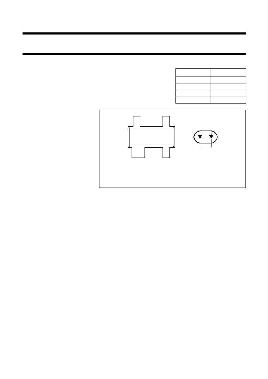
PINNING
PIN
DESCRIPTION
1
cathode (k1)
2
cathode (k2)
3
anode (a2)
4
anode (a1)
Fig.1 Simplified outline (SOT143) and symbol.
Marking code: L51.
handbook, halfpage
4
3
2
1
Top view
MAM059
2
3
4
1

1996 Sep 10
3
Philips Semiconductors
Product specification
High-speed double diode
BAS56
LIMITING VALUES
In accordance with the Absolute Maximum Rating System (IEC 134).
Note
1. Device mounted on an FR4 printed-circuit board.
SYMBOL
PARAMETER
CONDITIONS
MIN.
MAX.
UNIT
V
RRM
repetitive peak reverse voltage
-
60
V
V
RRM
repetitive peak reverse voltage
series connection
120
V
V
R
continuous reverse voltage
-
60
V
V
R
continuous reverse voltage
series connection
-
120
V
I
F
continuous forward current
single diode loaded; see Fig.2;
note 1
-
200
mA
double diode loaded; see Fig.2;
note 1
-
150
mA
I
FRM
repetitive peak forward current
single diode loaded
-
600
mA
double diode loaded
-
430
mA
I
FSM
non-repetitive peak forward current
square wave; T
j
= 25
∞
C prior to
surge; see Fig.4
t = 1
µ
s
-
9
A
t = 100
µ
s
-
3
A
t = 10 ms
-
1.7
A
P
tot
total power dissipation
T
amb
= 25
∞
C; note 1
-
250
mW
T
stg
storage temperature
-
65
+150
∞
C
T
j
junction temperature
-
150
∞
C

1996 Sep 10
4
Philips Semiconductors
Product specification
High-speed double diode
BAS56
ELECTRICAL CHARACTERISTICS
T
j
= 25
∞
C; unless otherwise specified.
Note
1. T
amb
= 25
∞
C; device has reached the thermal equilibrium when mounted on an FR4 printed-circuit board.
THERMAL CHARACTERISTICS
Note
1. Device mounted on an FR4 printed-circuit board.
SYMBOL
PARAMETER
CONDITIONS
MIN.
MAX.
UNIT
V
F
forward voltage
see Fig.3; I
F
= 200 mA; DC value;
note 1
-
1.0
V
I
R
reverse current
see Fig.5
V
R
= 60 V
-
100
nA
V
R
= 60 V; T
j
= 150
∞
C
-
100
µ
A
I
R
reverse current
series connection
-
V
R
= 120 V
-
100
nA
V
R
= 120 V; T
j
= 150
∞
C
-
100
µ
A
C
d
diode capacitance
f = 1 MHz; V
R
= 0; see Fig.6
-
2.5
pF
t
rr
reverse recovery time
when switched from I
F
= 400 mA to
I
R
= 400 mA; R
L
= 100
;
measured at I
R
= 40 mA; see Fig.7
-
6
ns
V
fr
forward recovery voltage
when switched from I
F
= 400 mA;
t
r
= 30 ns; see Fig.8
-
2.0
V
when switched from I
F
= 400 mA;
t
r
= 100 ns; see Fig.8
-
1.5
V
SYMBOL
PARAMETER
CONDITIONS
VALUE
UNIT
R
th j-tp
thermal resistance from junction to tie-point
360
K/W
R
th j-a
thermal resistance from junction to ambient
note 1
500
K/W
1996 Sep 10
5
Philips Semiconductors
Product specification
High-speed double diode
BAS56
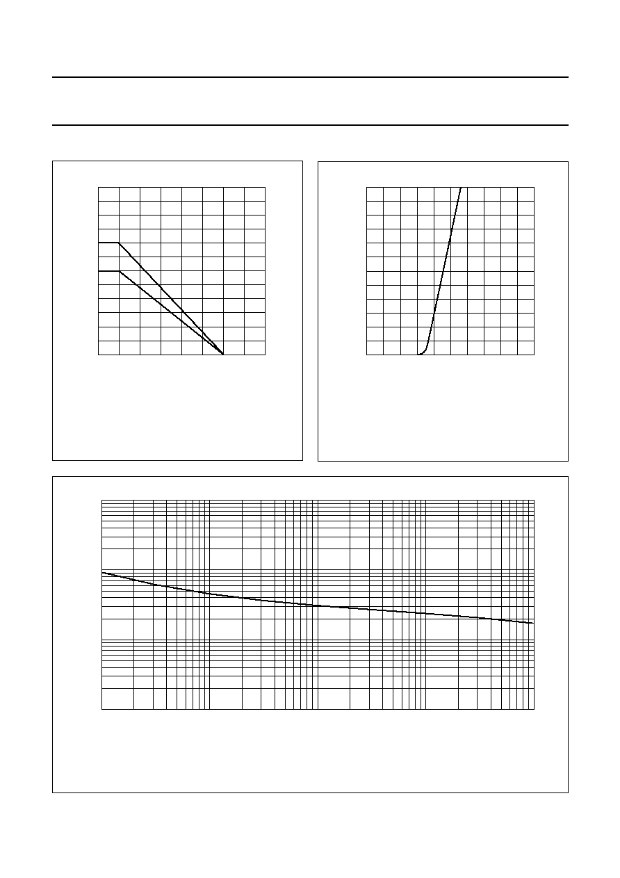
GRAPHICAL DATA
Fig.2
Maximum permissible continuous forward
current as a function of ambient temperature.
handbook, halfpage
0
100
(1)
(2)
200
300
200
0
100
MBG439
Tamb (
o
C)
IF
(mA)
Device mounted on a FR4 printed-circuit board.
(1) Single diode loaded.
(2) Double diode loaded.
Fig.3
Forward current as a function of forward
voltage; typical values.
handbook, halfpage
0
2
300
0
100
200
MBH279
1
IF
(mA)
VF (V)
T
j
= 25
∞
C.
Fig.4 Maximum permissible non-repetitive peak forward current as a function of pulse duration.
handbook, full pagewidth
MBG703
10
tp (
µ
s)
1
IFSM
(A)
10
2
10
-
1
10
4
10
2
10
3
10
1
Based on square wave currents.
T
j
= 25
∞
C prior to surge.