BCW61 Series
Vishay Semiconductors
formerly General Semiconductor
Document Number 88171
www.vishay.com
09-May-02
1
New Product
Small Signal Transistors (PNP)
Features
∑ PNP Silicon Epitaxial Planar Transistors
∑ Suited for low level, low noise, low
frequency applications in hybrid cicuits.
∑ Low Current, Low Voltage.
∑ As complementary types, BCW60 Series NPN
transistors are recommended.
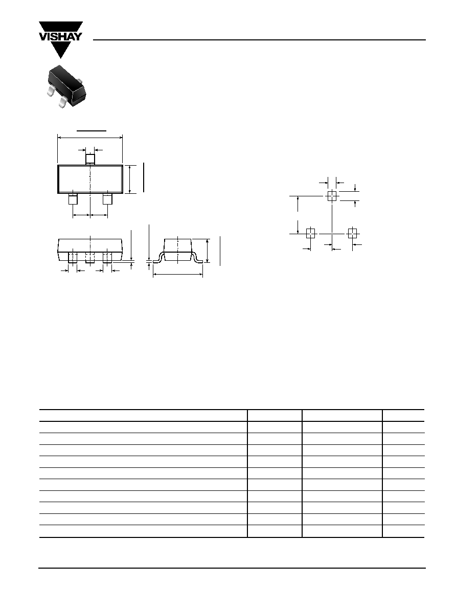
Mechanical Data
Case: SOT-23 Plastic Package
Weight: approx. 0.008g
Marking
BCW61A = BA
Code:
BCW61B = BB
BCW61C = BC
BCW61D = BD
Packaging Codes/Options:
E8/10K per 13" reel (8mm tape), 30K/box
E9/3K per 7" reel (8mm tape), 30K/box
.016 (0.4)
.056 (
1
.43
)
.037(0.95) .037(0.95)
ma
x
.
.004
(
0.1
)
.122 (3.1)
.016 (0.4)
.016 (0.4)
1
2
3
Top View
.102 (2.6)
.007 (
0
.17
5)
.0
45 (
1
.15)
.110 (2.8)
.052 (
1
.33
)
.005
(
0
.1
25)
.094 (2.4)
.0
37 (
0
.95)
TO-236AB (SOT-23)
Dimensions in inches and (millimeters)
Maximum Ratings & Thermal Characteristics
Ratings at 25∞C ambient temperature unless otherwise specified.
Parameter
Symbol
Value
Unit
Collector-Emitter Voltage (V
BE
= 0)
≠V
CES
32
V
Collector-Emitter Voltage
≠V
CEO
32
V
Emitter-Base Voltage
≠V
EBO
5.0
V
Collector Current (DC)
≠I
C
100
mA
Peak Collector Current
≠I
CM
200
mA
Base Current (DC)
≠I
B
50
mA
Power Dissipation
P
tot
250
mW
Maximum Junction Temperature
T
j
150
∞C
Storage Temperature Range
T
STG
≠65 to +150
∞C
Thermal Resistance, Junction to Ambient Air
R
JA
500
(1)
∞
C/W
Note:
(1) Mounted on FR-4 printed-ciruit board.
0.079 (2.0)
0.037 (0.95)
0.035 (0.9)
0.031 (0.8)
0.037 (0.95)
Mounting Pad Layout
Pin Configuration
1. Base
2. Emitter
3. Collector
BCW61 Series
Vishay Semiconductors
formerly General Semiconductor
www.vishay.com
Document Number 88171
2
09-May-02
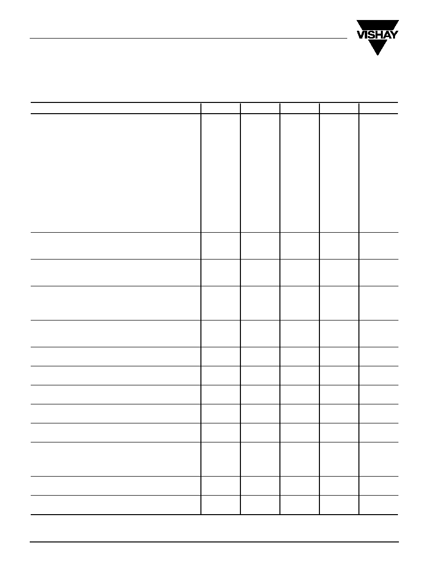
Electrical Characteristics
Ratings at 25∞C ambient temperature unless otherwise specified.
Symbol
Min.
TYP.
Max.
Unit
DC Current Gain
at ≠V
CE
= 5 V, ≠I
C
= 10
µ
A
BCW61A
h
FE
≠
≠
≠
≠
at ≠V
CE
= 5 V, ≠I
C
= 10
µ
A
BCW61B
h
FE
30
≠
≠
≠
at ≠V
CE
= 5 V, ≠I
C
= 10
µ
A
BCW61C
h
FE
40
≠
≠
≠
at ≠V
CE
= 5 V, ≠I
C
= 10
µ
A
BCW61D
h
FE
100
≠
≠
≠
at ≠V
CE
= 5 V, ≠I
C
= 2 mA
BCW61A
h
FE
120
≠
220
≠
at ≠V
CE
= 5 V, ≠I
C
= 2 mA
BCW61B
h
FE
180
≠
310
≠
at ≠V
CE
= 5 V, ≠I
C
= 2 mA
BCW61C
h
FE
250
≠
460
≠
at ≠V
CE
= 5 V, ≠I
C
= 2 mA
BCW61D
h
FE
380
≠
630
≠
at ≠V
CE
= 1 V, ≠I
C
= 50 mA
BCW61A
h
FE
60
≠
≠
≠
at ≠V
CE
= 1 V, ≠I
C
= 50 mA
BCW61B
h
FE
80
≠
≠
≠
at ≠V
CE
= 1 V, ≠I
C
= 50 mA
BCW61C
h
FE
100
≠
≠
≠
at ≠V
CE
= 1 V, ≠I
C
= 50 mA
BCW61D
h
FE
110
≠
≠
≠
Collector-Emitter Saturation Voltage
at ≠I
C
= 10 mA, ≠I
B
= 0.25 mA
≠V
CEsat
60
≠
250
mV
at ≠I
C
= 50 mA, ≠I
B
= 1.25 mA
≠V
CEsat
120
≠
550
mV
Base-Emitter Saturation Voltage
at ≠I
C
= 10 mA, ≠I
B
= 0.25 mA
≠V
BEsat
600
≠
850
mV
at ≠I
C
= 50 mA, ≠I
B
= 1.25 mA
≠V
BEsat
680
≠
1050
mV
Base-Emitter Voltage
at ≠V
CE
= 5 V, ≠I
C
= 2 mA
≠V
BE
600
650
750
mV
at ≠V
CE
= 5 V, ≠I
C
= 10
µ
A
≠V
BE
≠
550
≠
mV
at ≠V
CE
= 1 V, ≠I
C
= 50 mA
≠V
BE
≠
720
≠
mV
Collector-Emiter Cut-off Current
at ≠V
CE
= 32 V, V
EB
=0
≠I
CES
≠
≠
20
nA
at ≠V
CE
= 32 V, V
EB
=0, T
A
= 150
∞
C
≠
≠
20
µ
A
Emitter-Base Cut-off Current
at ≠V
EB
= 4 V, I
C
=0
≠I
EBO
≠
≠
20
nA
Gain-Bandwidth Product
at ≠V
CE
= 5 V, ≠I
C
= 10 mA, f = 100 MHz
f
T
100
≠
≠
MHz
Collector-Base Capacitance
at ≠V
CB
= 10 V, f = 1 MH
Z,
I
E
=0
C
CBO
≠
4.5
≠
pF
Emitter-Base Capacitance
at ≠V
EB
= 0.5 V, f = 1 MH
Z,
I
C
=0
C
EBO
≠
11
≠
pF
Noise Figure
at ≠V
CE
= 5 V, ≠I
C
= 200
µ
A, R
S
= 2 k
, f = 100 kH
Z
, B = 200Hz
F
≠
2
6
dB
Small Signal Current Gain
BCW60A
≠
200
at ≠V
CE
= 5V, ≠I
C
= 2 mA, f = 1.0 kH
Z
BCW60B
≠
260
BCW60C
h
fe
≠
330
BCW60D
≠
520
Turn-on Time at R
L
= 990
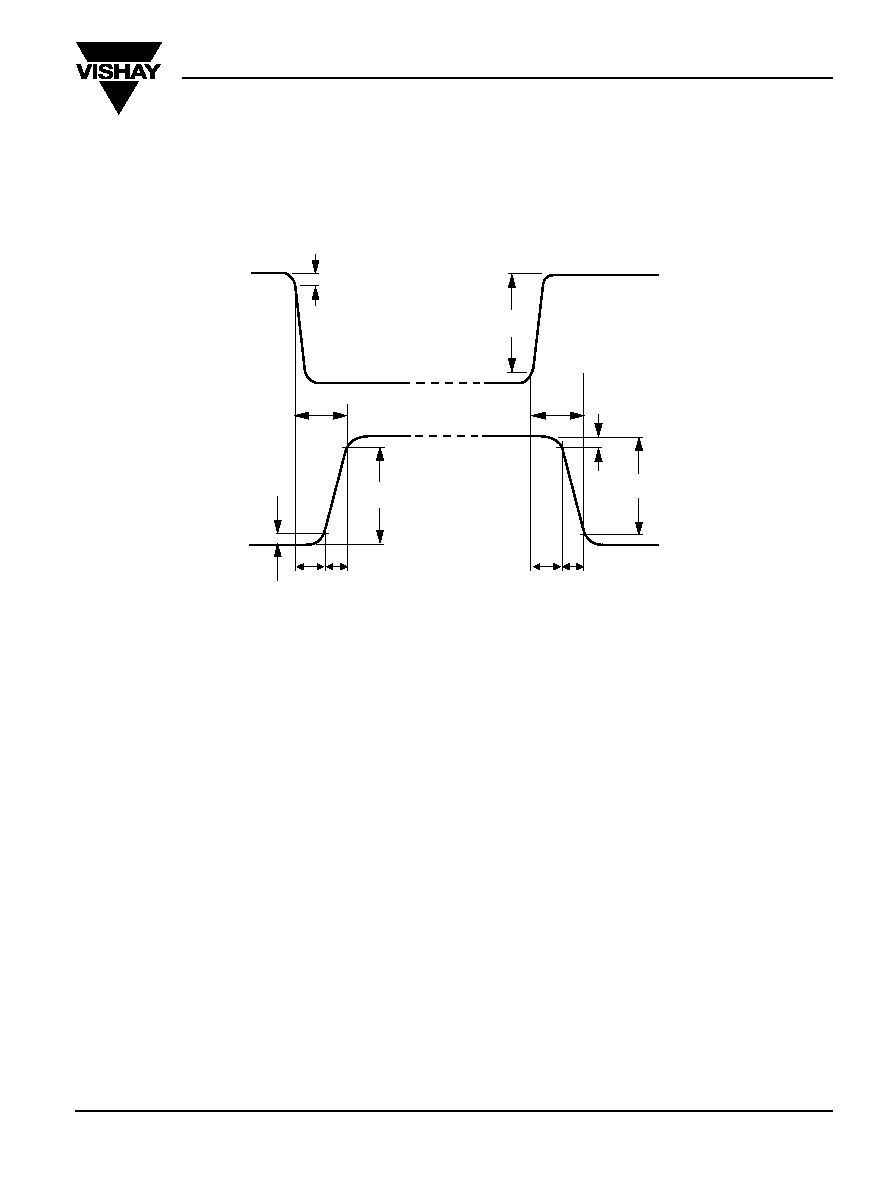
(see fig. 1)
≠ V
CC
= 10V, ≠Ic = 10mA, ≠I
B(on)
= I
B(off)
= 1mA
t
on
≠
85
150
ns
Turn-off Time at R
L
= 990
(see fig. 1)
≠ V
CC
= 10V, ≠Ic = 10mA, ≠I
B(on)
= I
B(off)
= 1mA
t
off
≠
480
800
ns