 | ÐлекÑÑоннÑй компоненÑ: BF961 | СкаÑаÑÑ:  PDF PDF  ZIP ZIP |
Äîêóìåíòàöèÿ è îïèñàíèÿ www.docs.chipfind.ru
BF961
Document Number 85002
Rev. 1.5, 25-Nov-04
Vishay Semiconductors
www.vishay.com
1
13625
1
4
3
2
G2
G1
D
S
Electrostatic sensitive device.
Observe precautions for handling.
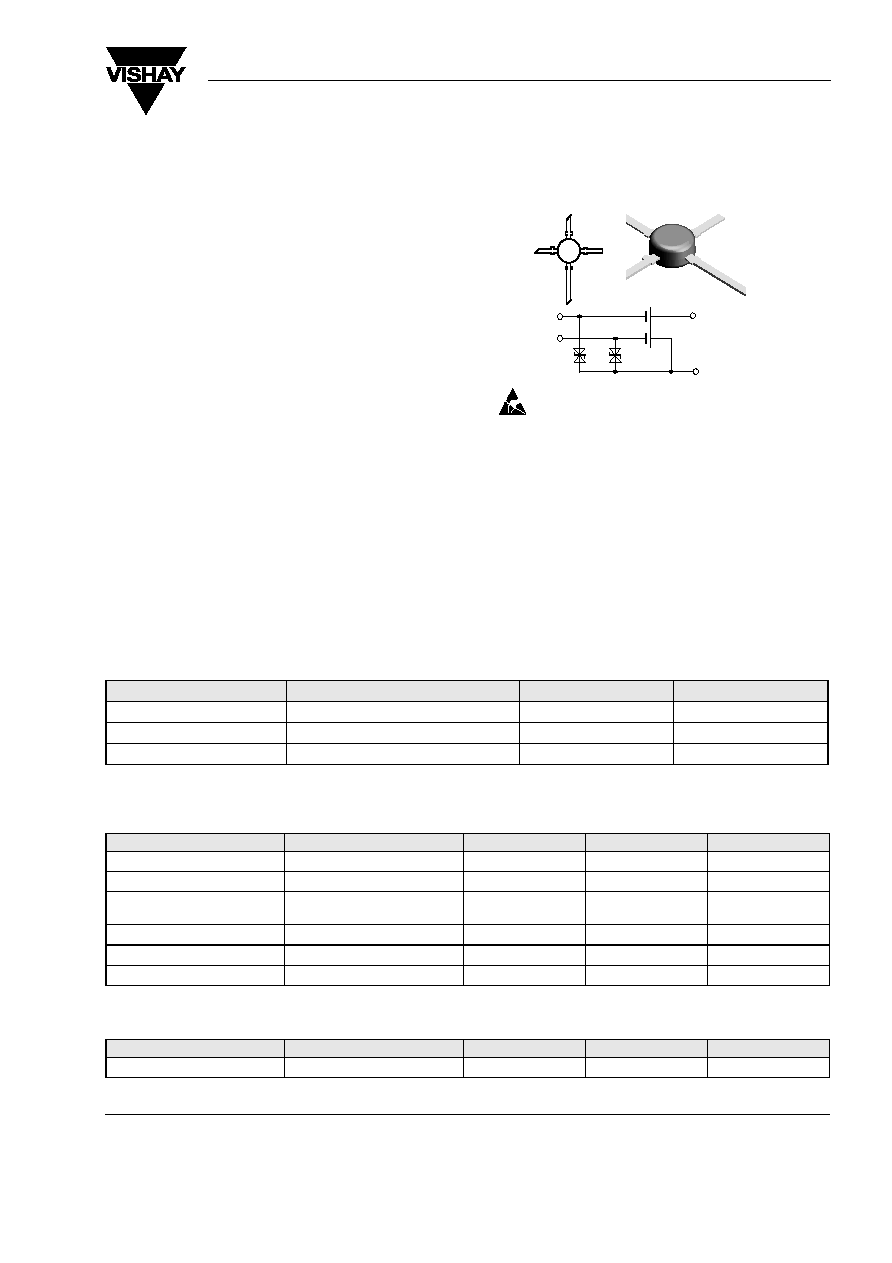
N-Channel Dual Gate MOS-Fieldeffect Tetrode, Depletion Mode
Features
· Integrated gate protection diodes
· High cross modulation performance
· Low noise figure
· High AGC-range
· Low feedback capacitance
· Low input capacitance
Applications
Input- and mixer stages especially for FM- and VHF
TV-tuners up to 300 MHz.
Mechanical Data
Case: TO-50 Plastic case
Weight: approx. 124 mg
Marking: BF961
Pinning:
1 = Drain, 2 = Source,
3 = Gate 1, 4 = Gate 2
Parts Table
Absolute Maximum Ratings
T
amb
= 25 °C, unless otherwise specified
Maximum Thermal Resistance
1)
on glass fibre printed board (40 x 25 x 1.5) mm
3
plated with 35
µm Cu
Part
Ordering Ccode
Marking
Package
BF961
BF961A or BF961B
BF961
TO50
BF961A
BF961A
BF961
TO50
BF961B
BF961B
BF961
TO50
Parameter
Test condition
Symbol
Value
Unit
Drain - source voltage
V
DS
20
V
Drain current
I
D
30
mA
Gate 1/Gate 2 - source peak
current
± I
G1/G2SM
10
mA
Total power dissipation
T
amb
60 °C
P
tot
200
mW
Channel temperature
T
Ch
150
°C
Storage temperature range
T
stg
- 55 to + 150
°C
Parameter
Test condition
Symbol
Value
Unit
Channel ambient
1)
R
thChA
450
K/W
www.vishay.com
2
Document Number 85002
Rev. 1.5, 25-Nov-04
VISHAY
BF961
Vishay Semiconductors
Electrical DC Characteristics
T
amb
= 25 °C, unless otherwise specified
Electrical AC Characteristics
T
amb
= 25 °C, unless otherwise specified
V
DS
= 15 V, I
D
= 10 mA, V
G2S
= 4 V, f = 1 MHz
Typical Characteristics (Tamb = 25
°C unless otherwise specified)
Parameter
Test condition
Part
Symbol
Min
Typ.
Max
Unit
Drain - source breakdown
voltage
I
D
= 10
µA, - V
G1S
= - V
G2S
= 4 V
V
(BR)DS
20
V
Gate 1 - source breakdown
voltage
± I
G1S
= 10 mA, V
G2S
= V
DS
= 0
± V
(BR)G1SS
8
14
V
Gate 2 - source breakdown
voltage
± I
G2S
= 10 mA, V
G1S
= V
DS
= 0
± V
(BR)G2SS
8
14
V
Gate 1 - source leakage current ± V
G1S
= 5 V, V
G2S
= V
DS
= 0
± I
G1SS
100
nA
Gate 2 - source leakage current ± V
G2S
= 5 V, V
G1S
= V
DS
= 0
± I
G2SS
100
nA
Drain current
V
DS
= 15 V, V
G1S
= 0, V
G2S
= 4 V BF961
I
DSS
4
20
mA
BF961A
I
DSS
4
10.5
mA
BF961B
I
DSS
9.5
20
mA
Gate 1 - source cut-off voltage
V
DS
= 15 V, V
G2S
= 4 V,
I
D
= 20
µA
- V
G1S(OFF)
3.5
V
Gate 2 - source cut-off voltage
V
DS
= 15 V, V
G1S
= 0, I
D
= 20
µA
- V
G2S(OFF)
3.5
V
Parameter
Test condition
Symbol
Min
Typ.
Max
Unit
Forward transadmittance
| y
21s
|
12
15
mS
Gate 1 input capacitance
C
issg1
3.7
pF
Gate 2 input capacitance
V
G1S
= 0, V
G2S
= 4 V
C
issg2
1.6
pF
Feedback capacitance
C
rss
25
fF
Output capacitance
C
oss
1.6
pF
Power gain
G
S
= 2 mS, G
L
= 0.5 mS,
f = 200 MHz
G
ps
20
dB
AGC range
V
G2S
= 4 to - 2 V, f = 200 MHz
G
ps
50
dB
Noise figure
G
S
= 2 mS, G
L
= 0.5 mS,
f = 200 MHz
F
1.8
2.5
dB
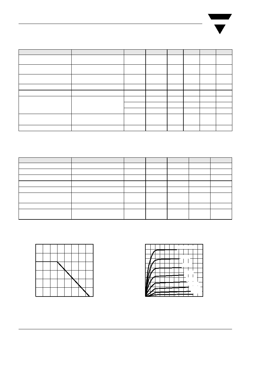
Figure 1. Total Power Dissipation vs. Ambient Temperature
0
50
100
150
200
250
300
0
20
40
60
80
100 120 140 160
96 12159
P
-
Total
Power
Dissipation
(
m
W
)
tot
T
amb
- Ambient Temperature (
°C )
Figure 2. Drain Current vs. Drain Source Voltage
0
2
4
6
8
10
12
14
16
18
20
22
0
2
4
6
8 10 12 14 16 18 20 22 24
V
DS
Drain Source Voltage ( V )
96 12160
I
Drain
Current
(
m
A
)
D
V
G1S
= 0.6 V
0.4 V
0.2 V
0
0.2 V
0.4 V
0.6 V
0.8 V
VISHAY
BF961
Document Number 85002
Rev. 1.5, 25-Nov-04
Vishay Semiconductors
www.vishay.com
3
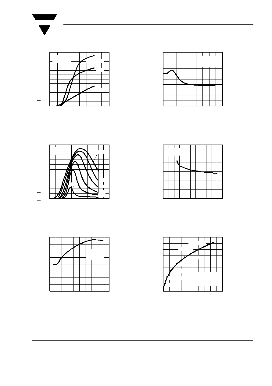
Figure 3. Forward Transadmittance vs. Gate 2 Source Voltage
Figure 4. Forward Transadmittance vs. Gate 1 Source Voltage
Figure 5. Gate 1 Input Capacitance vs. Gate 1 Source Voltage
0
2
4
6
8
10
12
14
16
18
20
22
24
2
1
0
1
2
3
4
5
6
V
G2S
Gate 2 Source Voltage ( V )
96 12161
Y
Forward
T
ransadmittance
(
m
S
)
21S
V
DS
= 15 V
I
DS
= 10 mA
V
G1S
= 0.5 V
0 V
0.5 V
0
2
4
6
8
10
12
14
16
18
20
22
-2 -1.5 -1 -0.5 0 0.5 1 1.5 2 2.5 3 3.5
V
G1S
- Gate 1 Source Voltage ( V )
96 12162
Y
Forward
T
ransadmittance
(
m
S
)
21S
V
DS
= 15 V
f = 1 MHz
V
G2S
= 5 V
4 V
3 V
2 V
1 V
0 V
0.0
0.5
1.0
1.5
2.0
2.5
3.0
3.5
4.0
2.01.51.00.5 0.0 0.5 1.0 1.5 2.0 2.5 3.0
V
G1S
Gate 1 Source Voltage ( V )
96 12163
C
Gate
1
Input
Capacitance
(
p
F
)
issg1
V
DS
= 15 V
V
G2S
= 4 V
f = 1 MHz
Figure 6. Gate 2 Input Capacitance vs. Gate 2 Source Voltage
Figure 7. Output Capacitance vs. Drain Source Voltage
Figure 8. Short Circuit Input Admittance
0.0
0.4
0.8
1.2
1.6
2.0
2.4
2.8
3.2
3.6
4.0
2
1
0
1
2
3
4
5
6
7
V
G2S
Gate 2 Source Voltage ( V )
96 12164
C
Gate
2
Input
Capacitance
(
p
F
)
issg2
V
DS
= 15 V
V
G1S
= 0
f = 1 MHz
0.0
0.5
1.0
1.5
2.0
2.5
3.0
0
2
4
6
8 10 12 14 16 18 20 22
V
DS
- Drain Source V oltage ( V )
96 12165
C
Output
Capacitance
(
p
F
)
oss
V
G2S
= 4 V
f = 1 MHz
0
2
4
6
8
10
12
14
16
18
0
1
2
3
4
5
6
7
8
9
10
Re (y
11
) ( mS )
96 12166
I
m(y
)
(
m
S
)
11
V
DS
= 15 V
V
G2S
= 4 V
I
D
= 5...20 mA
f = 50...700 MHz
f =700 MHz
600 MHz
500 MHz
400 MHz
300 MHz
200 MHz
100 MHz
www.vishay.com
4
Document Number 85002
Rev. 1.5, 25-Nov-04
VISHAY
BF961
Vishay Semiconductors
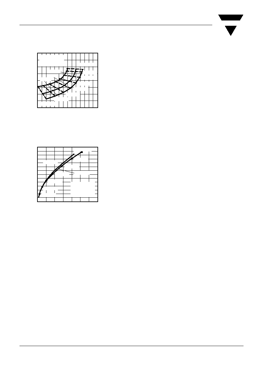
Figure 9. Short Circuit Forward Transfer Admittance
Figure 10. Short Circuit Output Admittance
30
25
20
15
10
5
0
5
10
0 2 4 6 8 10 12 14 16 18 20 22 24 26 28
Re (y
21
) ( mS )
96 12167
I
m(y
)
(
m
S
)
21
V
DS
= 15 V
V
G2S
= 4 V
f = 50...700 MHz
f = 50 MHz
600 MHz
500 MHz
400 MHz
300 MHz
200 MHz
100 MHz
700 MHz
I
D
= 5 mA
10 mA
20 mA
0.0
0.5
1.0
1.5
2.0
2.5
3.0
3.5
4.0
4.5
5.0
5.5
6.0
6.5
7.0
0.0
0.2
0.4
0.6
0.8
1.0
1.2
1.4
Re (y
22
) ( mS )
96 12168
I
m(y
)
(
m
S
)
22
V
DS
= 15 V
V
G2S
= 4 V
I
D
= 5...20 mA
f = 50...700 MHz
f = 700 MHz
600 MHz
500 MHz
400 MHz
300 MHz
200 MHz
100 MHz
I
D
= 5 mA
I
D
= 20 mA
VISHAY
BF961
Document Number 85002
Rev. 1.5, 25-Nov-04
Vishay Semiconductors
www.vishay.com
5
V
DS
= 15 V, I
D
= 5 to 20 mA, V
G2S
= 4 V, Z
0
= 50
S
11
S
21
S
12
S
22
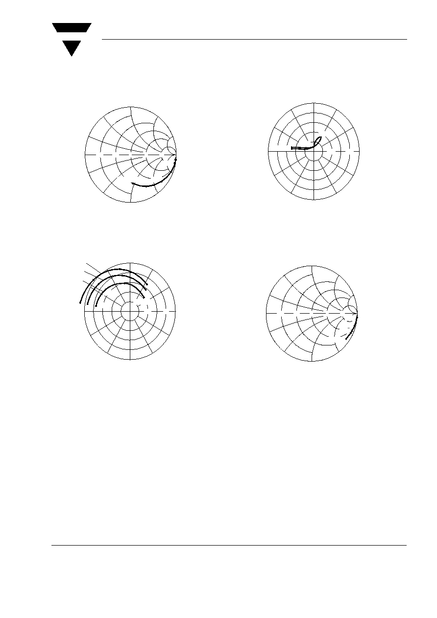
Figure 11. Input Reflection Coefficient
Figure 12. Forward Transmission Coefficient
j0.2
j0.5
j
j2
j5
0
j0.2
j0.5
j
j2
j5
0.2
0.5
1
2
5
700 MHz
100
50
300
500
12920
0 °
90°
180 °
90 °
0.8
1.6
150°
120°
60°
120°
60°
30°
12922
700MHz
200
400
50
30 °
I = 20 mA
D
I = 10 mA
D
I = 5 mA
D
Figure 13. Reverse Transmission Coefficient
Figure 14. Output Reflection Coefficient
700 MHz
12921
0 °
90 °
180°
90 °
0.04
0.08
150 °
120 °
60°
30°
120°
150°
60 °
30 °
600
300
12923
j0.2
j0.5
j
j2
j5
0
j0.2
j0.5
j
j2
j5
i
0.2
0.5
1
2
5
700 MHz
100
300
500

www.vishay.com
6
Document Number 85002
Rev. 1.5, 25-Nov-04
VISHAY
BF961
Vishay Semiconductors
Package Dimensions in mm
96 12242

VISHAY
BF961
Document Number 85002
Rev. 1.5, 25-Nov-04
Vishay Semiconductors
www.vishay.com
7
Ozone Depleting Substances Policy Statement
It is the policy of Vishay Semiconductor GmbH to
1. Meet all present and future national and international statutory requirements.
2. Regularly and continuously improve the performance of our products, processes, distribution and
operatingsystems with respect to their impact on the health and safety of our employees and the public, as
well as their impact on the environment.
It is particular concern to control or eliminate releases of those substances into the atmosphere which are
known as ozone depleting substances (ODSs).
The Montreal Protocol (1987) and its London Amendments (1990) intend to severely restrict the use of ODSs
and forbid their use within the next ten years. Various national and international initiatives are pressing for an
earlier ban on these substances.
Vishay Semiconductor GmbH has been able to use its policy of continuous improvements to eliminate the use
of ODSs listed in the following documents.
1. Annex A, B and list of transitional substances of the Montreal Protocol and the London Amendments
respectively
2. Class I and II ozone depleting substances in the Clean Air Act Amendments of 1990 by the Environmental
Protection Agency (EPA) in the USA