 | –≠–ª–µ–∫—Ç—Ä–æ–Ω–Ω—ã–π –∫–æ–º–ø–æ–Ω–µ–Ω—Ç: BF988 | –°–∫–∞—á–∞—Ç—å:  PDF PDF  ZIP ZIP |
BF988
Vishay Telefunken
www.vishay.de
∑
FaxBack +1-408-970-5600
Rev. 4, 08-Jul-99
1 (8)
Document Number 85007
N≠Channel Dual Gate MOS-Fieldeffect Tetrode,
Depletion Mode
Electrostatic sensitive device.
Observe precautions for handling.
Applications
Input- and mixer stages especially VHF- and UHF- tuners.
Features
D
Integrated gate protection diodes
D
High cross modulation performance
D
Low noise figure
D
High gain
D
High AGC-range
D
Low feedback capacitance
D
Low input capacitance
1
4
3
2
94 9307
96 12647
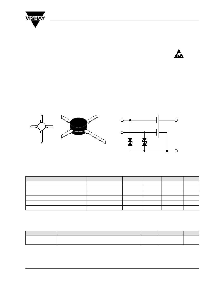
BF988 Marking: BF988
Plastic case (TO 50)
1 = Drain, 2 = Source, 3 = Gate 1, 4 = Gate 2
G
2
G
1
D
S
12623
Absolute Maximum Ratings
T
amb
= 25
_
C, unless otherwise specified
Parameter
Test Conditions
Type
Symbol
Value
Unit
Drain - source voltage
V
DS
12
V
Drain current
I
D
30
mA
Gate 1/Gate 2 - source peak current
±
I
G1/G2SM
10
mA
Total power dissipation
T
amb
60
∞
C
P
tot
200
mW
Channel temperature
T
Ch
150
∞
C
Storage temperature range
T
stg
≠55 to +150
∞
C
Maximum Thermal Resistance
T
amb
= 25
_
C, unless otherwise specified
Parameter
Test Conditions
Symbol
Value
Unit
Channel ambient
on glass fibre printed board (40 x 25 x 1.5) mm
3
plated with 35
m
m Cu
R
thChA
450
K/W
BF988
Vishay Telefunken
www.vishay.de
∑
FaxBack +1-408-970-5600
Rev. 4, 08-Jul-99
2 (8)
Document Number 85007
Electrical DC Characteristics
T
amb
= 25
_
C, unless otherwise specified
Parameter
Test Conditions
Type
Symbol
Min
Typ
Max
Unit
Drain - source
breakdown voltage
I
D
= 10
m
A,
≠V
G1S
= ≠V
G2S
= 4 V
V
(BR)DS
12
V
Gate 1 - source
breakdown voltage
±
I
G1S
= 10 mA,
V
G2S
= V
DS
= 0
±
V
(BR)G1SS
7
14
V
Gate 2 - source
breakdown voltage
±
I
G2S
= 10 mA,
V
G1S
= V
DS
= 0
±
V
(BR)G2SS
7
14
V
Gate 1 - source
leakage current
±
V
G1S
= 5 V,
V
G2S
= V
DS
= 0
±
I
G1SS
50
nA
Gate 2 - source
leakage current
±
V
G2S
= 5 V,
V
G1S
= V
DS
= 0
±
I
G2SS
50
nA
Drain current
V
DS
= 15 V, V
G1S
= 0,
BF988
I
DSS
4
18
mA
DS
G1S
V
G2S
= 4 V
BF988A
I
DSS
4
10.5
mA
BF988B
I
DSS
9.5
18
mA
Gate 1 - source
cut-off voltage
V
DS
= 15 V, V
G2S
= 4 V,
I
D
= 20
m
A
≠V
G1S(OFF)
2.5
V
Gate 2 - source
cut-off voltage
V
DS
= 15 V, V
G1S
= 0,
I
D
= 20
m
A
≠V
G2S(OFF)
2.0
V
Electrical AC Characteristics
V
DS
= 8 V, I
D
= 10 mA, V
G2S
= 4 V, f = 1 MHz , T
amb
= 25
_
C, unless otherwise specified
Parameter
Test Conditions
Type
Symbol
Min
Typ
Max
Unit
Forward transadmittance
y
21s
21
24
mS
Gate 1 input capacitance
C
issg1
2.1
2.5
pF
Gate 2 input capacitance
V
G1S
= 0, V
G2S
= 4 V
C
issg2
1.2
pF
Feedback capacitance
C
rss
25
fF
Output capacitance
C
oss
1.05
pF
Power gain
G
S
= 2 mS, G
L
= 0.5 mS,
f = 200 MHz
G
ps
28
dB
G
S
= 3,3 mS, G
L
= 1 mS,
f = 800 MHz
G
ps
16.5
20
dB
AGC range
V
G2S
= 4 to ≠2 V,
f = 800 MHz
D
G
ps
40
dB
Noise figure
G
S
= 2 mS, G
L
= 0.5 mS,
f = 200 MHz
F
1
dB
G
S
= 3,3 mS, G
L
= 1 mS,
f = 800 MHz
F
1.5
dB
BF988
Vishay Telefunken
www.vishay.de
∑
FaxBack +1-408-970-5600
Rev. 4, 08-Jul-99
3 (8)
Document Number 85007
Common Source S≠Parameters
V
DS
, = 8 V , V
G2S
= 4 V , Z
0
= 50
W,
T
amb
= 25
_
C, unless otherwise specified
S11
S21
S12
S22
I
D
/mA
f/MHz
LOG
MAG
ANG
LOG
MAG
ANG
LOG
MAG
ANG
LOG
MAG
ANG
dB
deg
dB
deg
dB
deg
dB
deg
100
≠0.02
≠7.8
6.01
168.4
≠56.27
83.0
≠0.02
≠3.6
200
≠0.10
≠15.3
5.87
156.3
≠50.61
76.6
≠0.06
≠7.3
300
≠0.31
≠22.8
5.69
144.2
≠47.70
70.9
≠0.13
≠10.6
400
≠0.56
≠30.2
5.42
132.9
≠46.19
65.6
≠0.20
≠14.2
500
≠0.87
≠37.3
5.17
121.5
≠45.46
60.6
≠0.28
≠17.5
600
≠1.26
≠44.3
4.85
110.6
≠45.84
55.4
≠0.36
20.5
5
700
≠1.59
≠50.9
4.54
100.4
≠47.31
58.6
≠0.43
≠23.8
800
≠2.04
≠58.0
4.25
90.2
≠48.19
63.3
≠0.49
≠26.8
900
≠2.42
≠64.4
4.02
80.6
≠50.37
81.5
≠0.52
≠30.2
1000
≠2.88
≠71.4
3.78
70.8
≠49.48
115.6
≠0.54
≠33.4
1100
≠3.39
≠78.3
3.42
60.5
47.92
131.7
≠0.66
≠36.8
1200
≠3.94
≠85.2
3.21
51.6
≠44.65
153.0
≠0.66
≠40.1
1300
≠4.46
≠91.8
3.01
42.0
≠41.76
159.8
≠0.66
≠43.9
100
≠0.02
≠8.3
7.84
168.5
≠55.67
83.0
≠0.04
≠3.7
200
≠0.11
≠16.1
7.70
156.6
≠50.01
76.4
≠0.09
≠7.4
300
≠0.35
≠24.0
7.49
144.8
≠47.20
70.3
≠0.16
≠10.8
400
≠0.62
≠31.6
7.21
133.6
≠45.60
65.1
≠0.23
≠14.3
500
≠0.97
≠39.2
6.93
122.5
≠44.88
60.0
≠0.31
17.9
600
≠1.39
≠46.4
6.59
111.9
≠45.25
54.5
≠0.42
≠20.9
10
700
≠1.76
≠53.2
6.27
101.9
≠46.51
57.4
≠0.48
≠24.1
800
≠2.25
≠60.3
5.97
92.1
≠47.19
61.4
≠0.55
≠27.3
900
≠2.67
≠67.1
5.71
82.8
≠49.28
76.0
≠0.58
≠30.6
1000
≠3.16
≠74.1
5.46
73.3
≠48.99
107.1
≠0.60
≠33.8
1100
≠3.72
≠81.1
5.07
63.3
≠48.03
123.3
≠0.73
≠37.2
1200
≠4.30
≠88.0
4.85
54.6
≠45.15
147.6
≠0.73
≠40.6
1300
≠4.87
≠94.4
4.63
45.4
≠42.46
157.0
≠0.73
≠44.3
100
≠0.01
≠8.4
8.62
168.6
≠55.26
83.0
≠0.07
≠3.7
200
≠0.13
≠16.4
8.46
156.8
≠49.61
76.3
≠0.12
≠7.5
3000
≠0.37
≠24.5
8.26
145.2
≠46.70
70.3
≠0.20
≠11.0
400
≠0.66
≠32.3
7.96
134.0
≠45.10
64.9
≠0.27
≠14.4
500
≠1.02
≠39.8
7.66
122.9
≠44.38
59.7
≠0.36
≠18.0
600
≠1.47
≠47.0
7.33
112.3
≠44.65
54.3
≠0.47
≠20.9
15
700
≠1.85
≠54.1
6.98
102.6
≠45.72
57.0
≠0.53
≠24.2
800
≠2.36
≠61.3
6.68
92.8
≠46.29
60.0
≠0.61
≠27.4
900
≠2.80
≠67.9
6.42
83.7
≠48.18
71.9
≠0.64
≠30.6
1000
≠3.30
≠75.0
6.15
74.3
≠48.49
98.7
≠0.66
≠33.9
1100
3.89
≠82.0
5.75
64.6
≠47.93
114.8
≠≠0.77
≠37.3
1200
≠4.49
≠88.8
5.52
56.0
≠45.75
141.2
≠0.79
≠40.8
1300
≠5.06
≠95.2
5.30
46.9
≠43.05
153.4
≠0.79
≠44.5
BF988
Vishay Telefunken
www.vishay.de
∑
FaxBack +1-408-970-5600
Rev. 4, 08-Jul-99
4 (8)
Document Number 85007
Typical Characteristics (T
amb
= 25
_
C unless otherwise specified)
0
50
100
150
200
250
300
0
20
40
60
80
100 120 140 160
T
amb
≠ Ambient Temperature (
∞
C )
96 12159
P
≠
T
otal Power Dissipation ( mW
)
tot
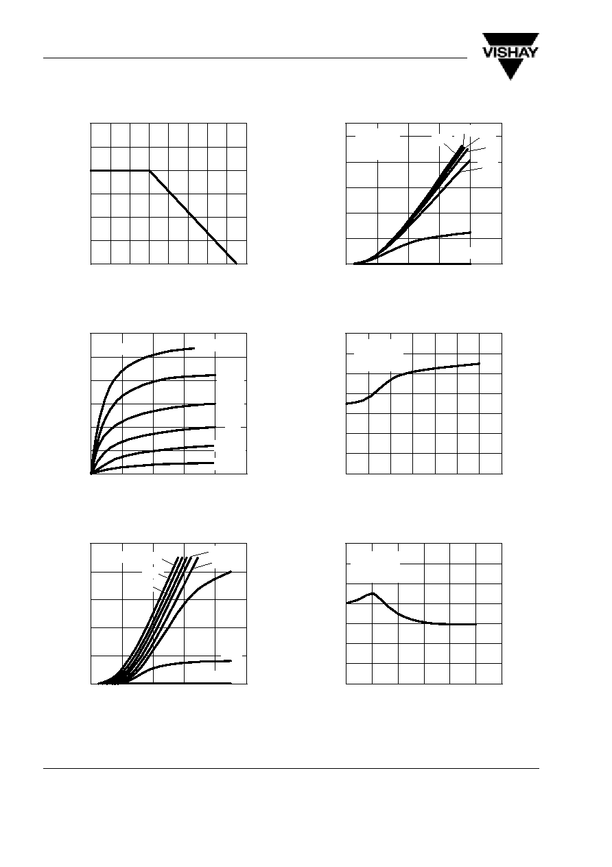
Figure 1. Total Power Dissipation vs.
Ambient Temperature
0
5
10
15
20
25
30
0
2
4
6
8
10
V
DS
≠ Drain Source Voltage ( V )
12812
I ≠ Drain Current ( mA
)
D
V
G1S
= 0.6V
0.4V
0
≠0.4V
0.2V
V
G2S
= 4V
≠0.2V
Figure 2. Drain Current vs.
Drain Source Voltage
0
4
8
12
16
20
≠0.8
≠0.4
0.0
0.4
0.8
1.2
V
G1S
≠ Gate 1 Source Voltage ( V )
12816
I ≠ Drain Current ( mA
)
D
6V
5V
4V
0
2V
1V
3V
V
DS
= 8V
V
G2S
=≠1V
Figure 3. Drain Current vs. Gate 1 Source Voltage
0
4
8
12
16
20
≠0.6
≠0.2
0.2
0.6
1.0
1.4
V
G2S
≠ Gate 2 Source Voltage ( V )
12817
I ≠ Drain Current ( mA
)
D
0
2V
1V
3V
V
DS
= 8V
5V
V
G1S
= ≠1V
4V
Figure 4. Drain Current vs. Gate 2 Source Voltage
0
0.4
0.8
1.2
1.6
2.0
2.4
2.8
≠2
≠1.5
≠1.0
≠0.5
0.0
0.5
1.0
1.5
V
G1S
≠ Gate 1 Source Voltage ( V )
12813
C ≠ Gate 1 Input Capacitance ( pF )
issg1
V
DS
=8V
V
G2S
=4V
f=1MHz
Figure 5. Gate 1 Input Capacitance vs.
Gate 1 Source Voltage
0
0.4
0.8
1.2
1.6
2.0
2.4
2.8
≠1
0
1
2
3
4
5
V
G2S
≠ Gate 2 Source Voltage ( V )
12814
C ≠ Gate 2 Input Capacitance ( pF )
issg2
V
DS
=8V
V
G1S
=0
f=1MHz
Figure 6. Gate 2 Input Capacitance vs.
Gate 2 Source Voltage

BF988
Vishay Telefunken
www.vishay.de
∑
FaxBack +1-408-970-5600
Rev. 4, 08-Jul-99
5 (8)
Document Number 85007
0
0.8
1.6
2.4
3.2
4.0
2
4
6
8
10
12
V
DS
≠ Drain Source Voltage ( V )
12815
C ≠ Output Capacitance ( pF )
oss
V
G2S
=4V
V
G1S
=0
f=1MHz
Figure 7. Output Capacitance vs. Drain Source Voltage
≠50
≠40
≠30
≠20
≠10
0
10
≠1
≠0.5
0.0
0.5
1.0
1.5
V
G1S
≠ Gate 1 Source Voltage ( V )
12818
S ≠
T
ransducer
Gain
(
dB
)
2
21
4V
0
2V
1V
3V
f= 800MHz
≠0.2V
V
G2S
=≠0.8V
≠0.4V
Figure 8. Transducer Gain vs. Gate 1 Source Voltage
0
4
8
12
16
20
24
28
32
0
4
8
12
16
20
24
28
I
D
≠ Drain Current ( mA )
12819
V
DS
=8V
f=1MHz
V
G2S
=4V
2V
1V
0
3V
y ≠ Forward
T
ransadmittance ( mS )
21s
Figure 9. Forward Transadmittance vs. Drain Current
0
2
4
6
8
10
12
14
16
18
20
0
2
4
6
8
10
12
14
Re (y
11
) ( mS )
12820
Im ( y ) ( mS )
11
V
DS
=8V
V
G2S
=4V
I
D
=10mA
f=100...1300MHz
f=1300MHz
700MHz
400MHz
1000MHz
100MHz
Figure 10. Short Circuit Input Admittance
≠40
≠35
≠30
≠25
≠20
≠15
≠10
≠5
0
5
0
4
8
12
16
20
24
28
32
Re (y
21
) ( mS )
12821
Im ( y ) ( mS )
21
V
DS
=8V
V
G2S
=4V
f=100...1300MHz
f=100MHz
1300MHz
1000MHz
400MHz
700MHz
I
D
=5mA
10mA
20mA
Figure 11. Short Circuit Forward Transfer Admittance
0
1
2
3
4
5
6
7
8
9
0
0.25
0.50
0.75
1.00
1.25
1.50
Re (y
22
) ( mS )
12822
Im ( y ) ( mS )
22
V
DS
=15V
V
G2S
=4V
I
D
=10mA
f=100...1300MHz
f=1300MHz
1000MHz
400MHz
100MHz
700MHz
Figure 12. Short Circuit Output Admittance