 | –≠–ª–µ–∫—Ç—Ä–æ–Ω–Ω—ã–π –∫–æ–º–ø–æ–Ω–µ–Ω—Ç: BF994 | –°–∫–∞—á–∞—Ç—å:  PDF PDF  ZIP ZIP |
BF994S
Vishay Telefunken
www.vishay.de
∑
FaxBack +1-408-970-5600
Rev. 3, 20-Jan-99
1 (7)
Document Number 85008
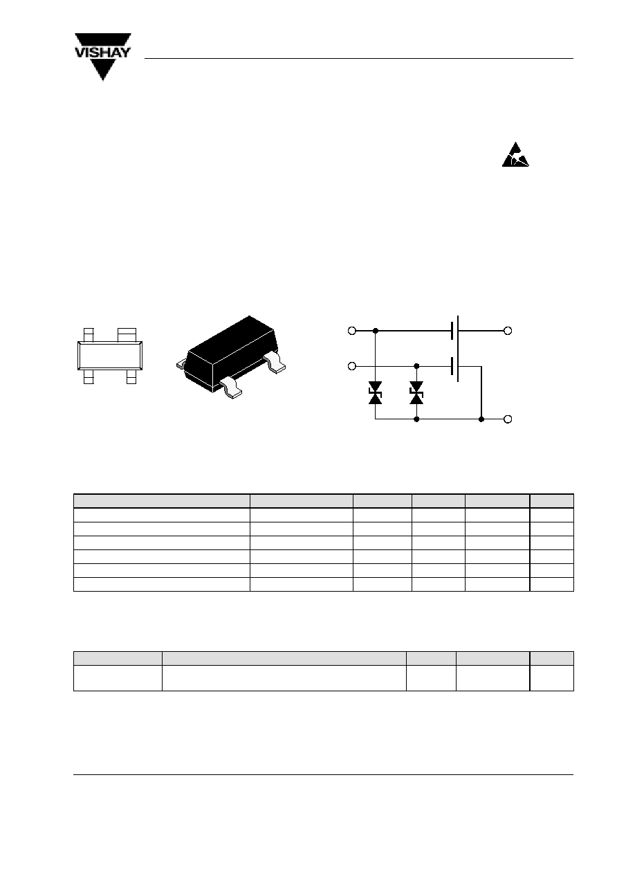
N≠Channel Dual Gate MOS-Fieldeffect Tetrode,
Depletion Mode
Electrostatic sensitive device.
Observe precautions for handling.
Applications
Input- and mixer stages especially VHF TV-tuners.
Features
D
Integrated gate protection diodes
D
High cross modulation performance
D
Low noise figure
D
High AGC-range
D
Low feedback capacitance
D
Low input capacitance
13 579
2
1
4
3
94 9279
BF994 Marking: MG
Plastic case (SOT 143)
1=Source, 2=Drain, 3=Gate 2, 4=Gate 1
G
2
G
1
D
S
12623
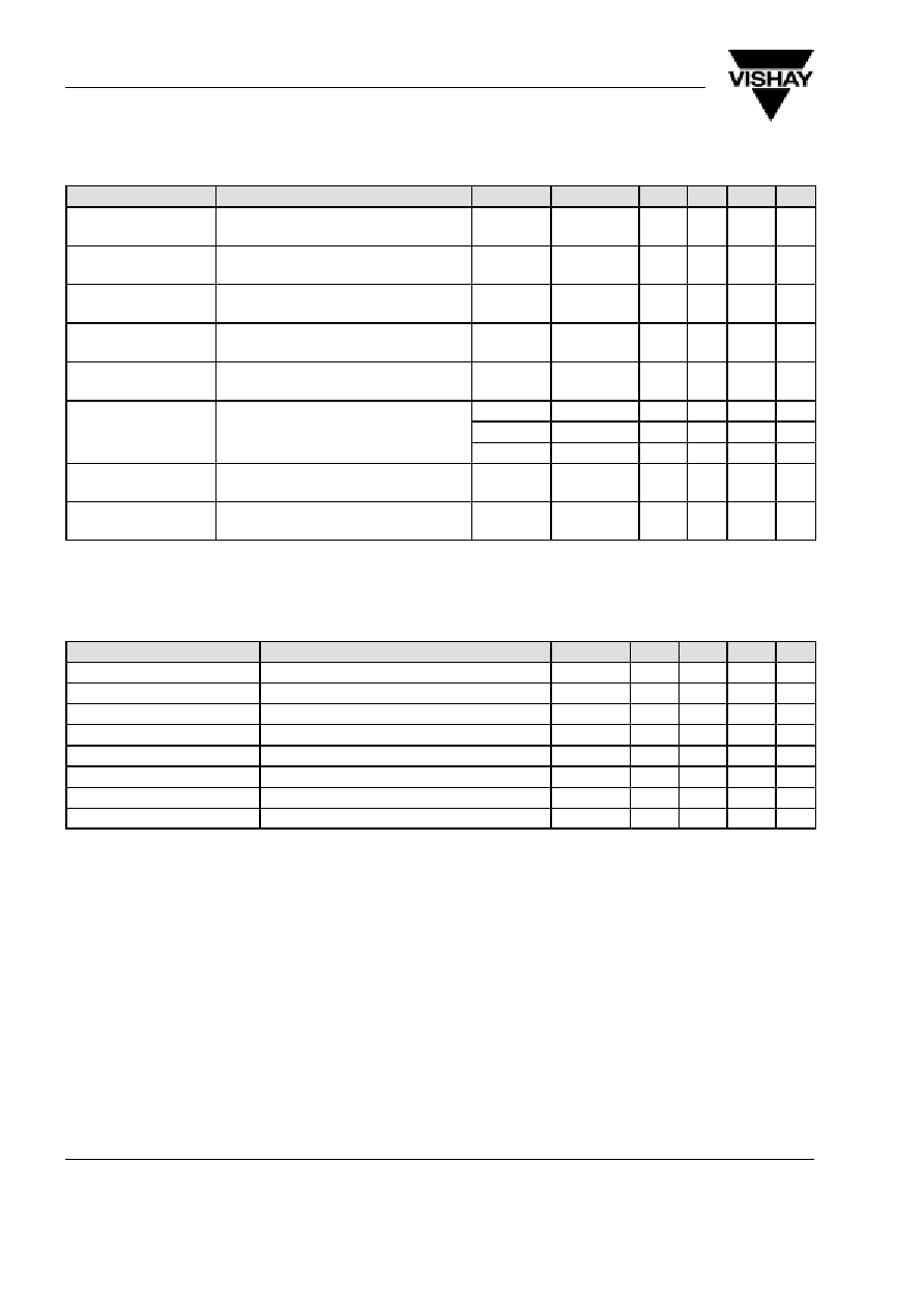
Absolute Maximum Ratings
T
amb
= 25
_
C, unless otherwise specified
Parameter
Test Conditions
Type
Symbol
Value
Unit
Drain - source voltage
V
DS
20
V
Drain current
I
D
30
mA
Gate 1/Gate 2 - source peak current
±
I
G1/G2SM
10
mA
Total power dissipation
T
amb
60
∞
C
P
tot
200
mW
Channel temperature
T
Ch
150
∞
C
Storage temperature range
T
stg
≠55 to +150
∞
C
Maximum Thermal Resistance
T
amb
= 25
_
C, unless otherwise specified
Parameter
Test Conditions
Symbol
Value
Unit
Channel ambient
on glass fibre printed board (25 x 20 x 1.5) mm
3
plated with 35
m
m Cu
R
thChA
450
K/W
BF994S
Vishay Telefunken
www.vishay.de
∑
FaxBack +1-408-970-5600
Rev. 3, 20-Jan-99
2 (7)
Document Number 85008
Electrical DC Characteristics
T
amb
= 25
_
C, unless otherwise specified
Parameter
Test Conditions
Type
Symbol
Min
Typ
Max
Unit
Drain - source
breakdown voltage
I
D
= 10
m
A, ≠V
G1S
= ≠V
G2S
= 4 V
V
(BR)DS
20
V
Gate 1 - source
breakdown voltage
±
I
G1S
= 10 mA, V
G2S
= V
DS
= 0
±
V
(BR)G1SS
6
20
V
Gate 2 - source
breakdown voltage
±
I
G2S
= 10 mA, V
G1S
= V
DS
= 0
±
V
(BR)G2SS
20
V
Gate 1 - source
leakage current
±
V
G1S
= 5 V, V
G2S
= V
DS
= 0
±
I
G1SS
50
nA
Gate 2 - source
leakage current
±
V
G2S
= 5 V, V
G1S
= V
DS
= 0
±
I
G2SS
50
nA
Drain current
V
DS
= 15 V, V
G1S
= 0, V
G2S
= 4 V
BF994S
I
DSS
4
18
mA
DS
G1S
G2S
BF994SA
I
DSS
4
10.5
mA
BF994SB
I
DSS
9.5
18
mA
Gate 1 - source
cut-off voltage
V
DS
= 15 V, V
G2S
= 4 V, I
D
= 20
m
A
≠V
G1S(OFF)
2.5
V
Gate 2 - source
cut-off voltage
V
DS
= 15 V, V
G1S
= 0, I
D
= 20
m
A
≠V
G2S(OFF)
2.0
V
Electrical AC Characteristics
V
DS
= 15 V, I
D
= 10 mA, V
G2S
= 4 V, f = 1 MHz , T
amb
= 25
_
C, unless otherwise specified
Parameter
Test Conditions
Symbol
Min
Typ
Max
Unit
Forward transadmittance
y
21s
15
18.5
mS
Gate 1 input capacitance
C
issg1
2.5
3.0
pF
Gate 2 input capacitance
V
G1S
= 0, V
G2S
= 4 V
C
issg2
1.2
pF
Feedback capacitance
C
rss
25
35
fF
Output capacitance
C
oss
1.0
1.3
pF
Power gain
G
S
= 2 mS, G
L
= 0.5 mS, f = 200 MHz
G
ps
25
dB
AGC range
V
G2S
= 4 to ≠2 V, f = 200 MHz
D
G
ps
50
dB
Noise figure
G
S
= 2 mS, G
L
= 0.5 mS, f = 200 MHz
F
1.0
dB
BF994S
Vishay Telefunken
www.vishay.de
∑
FaxBack +1-408-970-5600
Rev. 3, 20-Jan-99
3 (7)
Document Number 85008
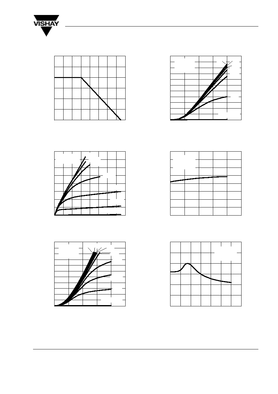
Typical Characteristics (T
amb
= 25
_
C unless otherwise specified)
0
50
100
150
200
250
300
0
20
40
60
80
100 120 140 160
T
amb
≠ Ambient Temperature (
∞
C )
96 12159
P
≠
T
otal Power Dissipation ( mW
)
tot
Figure 1. Total Power Dissipation vs.
Ambient Temperature
0
4
8
12
16
20
24
28
32
0
2
4
6
8
10
12
14
16
V
DS
≠ Drain Source Voltage ( V )
12849
I ≠ Drain Current ( mA
)
D
V
G1S
= ≠1V
1V
0
2V
0.5V
V
G2S
= 4V
P
tot
=200mW
≠0.5V
1.5V
Figure 2. Drain Current vs. Drain Source Voltage
0
2
4
6
8
10
12
14
16
18
20
22
≠1
≠0.5
0.0
0.5
1.0
1.5
V
G1S
≠ Gate 1 Source Voltage ( V )
12851
I ≠ Drain Current ( mA
)
D
V
G2S
= ≠1V
5V 4V
0
2V
1V
3V
V
DS
= 15V
6V
0.5V
Figure 3. Drain Current vs. Gate 1 Source Voltage
0
2
4
6
8
10
12
14
16
18
20
22
≠1
≠0.5
0.0
0.5
1.0
1.5
V
G2S
≠ Gate 2 Source Voltage ( V )
12852
I ≠ Drain Current ( mA
)
D
V
G1S
= ≠1V
0
2V
1V
3V
V
DS
= 15V
5V
4V
Figure 4. Drain Current vs. Gate 2 Source Voltage
0
0.5
1.0
1.5
2.0
2.5
3.0
3.5
4.0
≠1
≠0.5
0.0
0.5
1.0
1.5
I
D
≠ Drain Current ( mA )
12853
C ≠ Gate 1 Input Capacitance ( pF )
issg1
V
DS
=15V
V
G2S
=4V
f=1MHz
Figure 5. Gate 1 Input Capacitance vs. Drain Current
0
0.5
1.0
1.5
2.0
2.5
3.0
≠2
≠1
0
1
2
3
4
5
V
G2S
≠ Gate 2 Source Voltage ( V )
12854
C ≠ Gate 2 Input Capacitance ( pF )
issg2
V
DS
=15V
V
G1S
=0
f=1MHz
Figure 6. Gate 2 Input Capacitance vs.
Gate 2 Source Voltage
BF994S
Vishay Telefunken
www.vishay.de
∑
FaxBack +1-408-970-5600
Rev. 3, 20-Jan-99
4 (7)
Document Number 85008
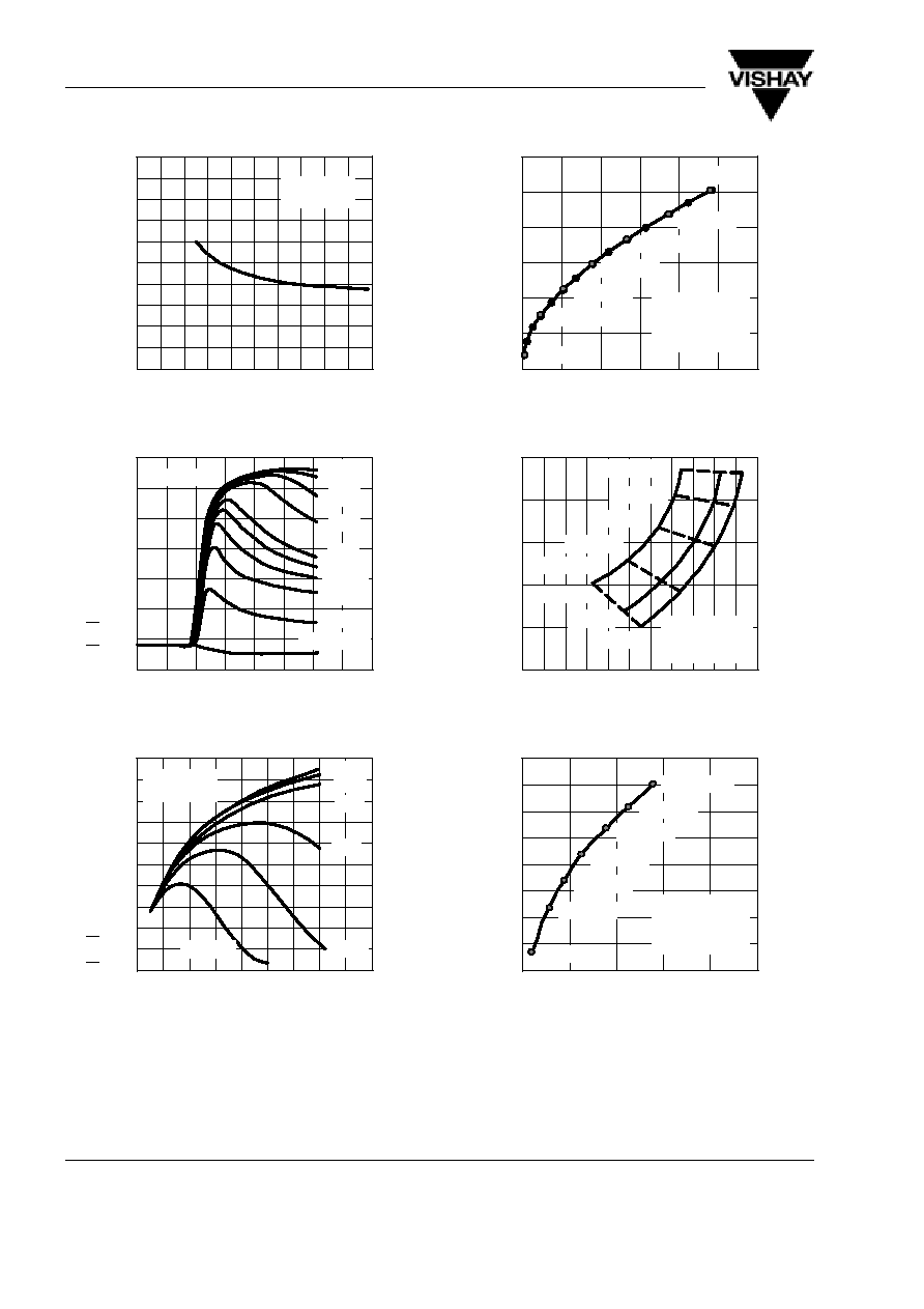
0
0.2
0.4
0.6
0.8
1.0
1.2
1.4
1.6
1.8
2.0
0
2
4
6
8
10 12 14 16 18 20
V
DS
≠ Drain Source Voltage ( V )
12856
C ≠ Output Capacitance ( pF )
oss
V
G2S
=4V
f=1MHz
Figure 7. Output Capacitance vs. Drain Source Voltage
≠60
≠50
≠40
≠30
≠20
≠10
0
10
≠2.0 ≠1.5 ≠1.0 ≠0.5 0.0
0.5
1.0
1.5
2.0
V
G1S
≠ Gate 1 Source Voltage ( V )
12855
S ≠
T
ransducer
Gain
(
dB
)
2
21
4V
0
2V
1V
3V
f= 200MHz
≠0.2V
V
G2S
=≠1V
≠0.8V
≠0.6V
≠0.4V
Figure 8. Transducer Gain vs. Gate 1 Source Voltage
0
2
4
6
8
10
12
14
16
18
20
0
2
4
6
8
10
12
14
16
18
I
D
≠ Drain Current ( mA )
12850
V
DS
=15V
f=1MHz
4V
2V
3V
1V
0.5V
V
G2S
=0
y ≠ Forward
T
ransadmittance ( mS )
21s
Figure 9. Forward Transadmittance vs. Drain Current
0
2
4
6
8
10
12
0
0.5
1.0
1.5
2.0
2.5
3.0
Re (y
11
) ( mS )
12860
Im ( y ) ( mS )
11
V
DS
=15V
V
G2S
=4V
I
D
=10mA
f=50...700MHz
f=700MHz
600MHz
500MHz
400MHz
300MHz
200MHz
50MHz
Figure 10. Short Circuit Input Admittance
≠20
≠16
≠12
≠8
≠4
0
0
2
4
6
8
10 12 14 16 18 20 22
Re (y
21
) ( mS )
12861
Im ( y ) ( mS )
21
V
DS
=15V
V
G2S
=4V
f=50...700MHz
f=50MHz
500MHz
300MHz
150MHz
700MHz
I
D
=5mA
10mA
20mA
Figure 11. Short Circuit Forward Transfer Admittance
0
0.5
1.0
1.5
2.0
2.5
3.0
3.5
4.0
0
0.4
0.8
1.2
1.6
2.0
Re (y
22
) ( mS )
12862
Im ( y ) ( mS )
22
V
DS
=15V
V
G2S
=4V
I
D
=10mA
f=50...700MHz
f=700MHz
600MHz
500MHz
400MHz
300MHz
200MHz
50MHz
Figure 12. Short Circuit Output Admittance
BF994S
Vishay Telefunken
www.vishay.de
∑
FaxBack +1-408-970-5600
Rev. 3, 20-Jan-99
5 (7)
Document Number 85008
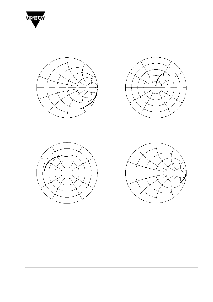
V
DS
= 15 V, I
D
= 10 mA, V
G2S
= 4 V , Z
0
= 50
W
S
11
12 964
≠j0.2
≠j0.5
≠j
≠j2
≠j5
0
j0.2
j0.5
j
j2
j5
1
¡¡¡
¡¡¡
0.2
¡¡
¡¡
0.5
¡¡
¡¡
1
¡¡
¡¡
2
¡¡
¡¡
5
50
700MHz
200
450
Figure 13. Input reflection coefficient
S
21
12 966
0
∞
90
∞
180
∞
≠90
∞
1
2
≠150
∞
≠120
∞
≠60
∞
≠30
∞
120
∞
150
∞
60
∞
30
∞
50
700MHz
200
450
Figure 14. Forward transmission coefficient
S
12
12 965
0
∞
90
∞
180
∞
≠90
∞
0.08
0.16
≠150
∞
≠120
∞
≠60
∞
≠30
∞
120
∞
150
∞
60
∞
30
∞
50
700MHz
200
Figure 15. Reverse transmission coefficient
S
22
12 967
≠j0.2
≠j0.5
≠j
≠j2
≠j5
0
j0.2
j0.5
j
j2
j5
1
¡¡¡
0.2
¡¡¡
0.5
¡¡
1
¡¡
2
¡¡
5
50
700MHz
Figure 16. Output reflection coefficient