 | ÐлекÑÑоннÑй компоненÑ: BF996SB | СкаÑаÑÑ:  PDF PDF  ZIP ZIP |
Äîêóìåíòàöèÿ è îïèñàíèÿ www.docs.chipfind.ru
BF996S
Vishay Telefunken
www.vishay.de
·
FaxBack +1-408-970-5600
Rev. 3, 20-Jan-99
1 (8)
Document Number 85010
NChannel Dual Gate MOS-Fieldeffect Tetrode,
Depletion Mode
Electrostatic sensitive device.
Observe precautions for handling.
Applications
Input- and mixer stages in UHF tuners.
Features
D
Integrated gate protection diodes
D
Low noise figure
D
Low feedback capacitance
D
High cross modulation performance
D
Low input capacitance
D
High AGC-range
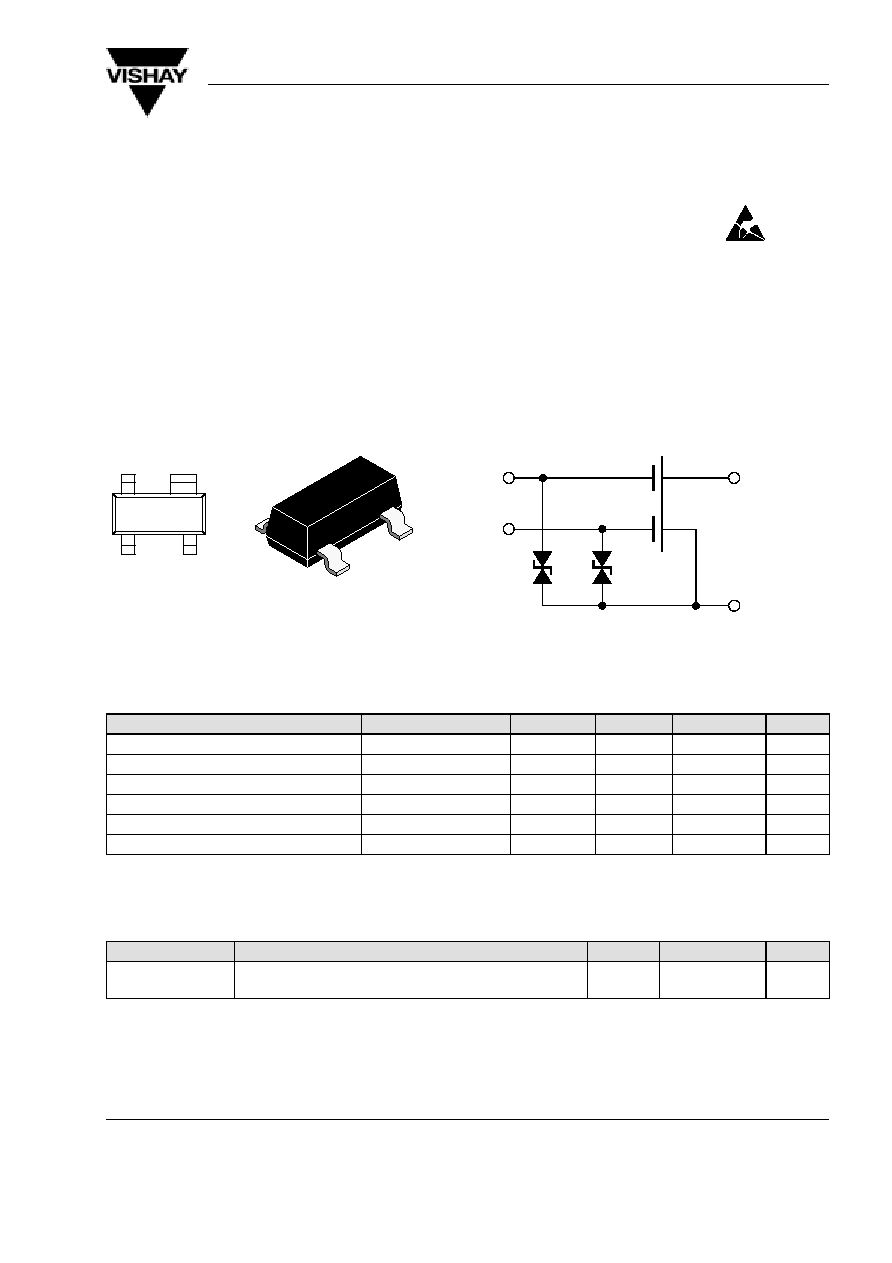
13 579
2
1
4
3
94 9279
BF996S Marking: MH
Plastic case (SOT 143)
1=Source, 2=Drain, 3=Gate 2, 4=Gate 1
G
2
G
1
D
S
12623
Absolute Maximum Ratings
T
amb
= 25
_
C, unless otherwise specified
Parameter
Test Conditions
Type
Symbol
Value
Unit
Drain - source voltage
V
DS
20
V
Drain current
I
D
30
mA
Gate 1/Gate 2 - source peak current
±
I
G1/G2SM
10
mA
Total power dissipation
T
amb
60
°
C
P
tot
200
mW
Channel temperature
T
Ch
150
°
C
Storage temperature range
T
stg
65 to +150
°
C
Maximum Thermal Resistance
T
amb
= 25
_
C, unless otherwise specified
Parameter
Test Conditions
Symbol
Value
Unit
Channel ambient
on glass fibre printed board (25 x 20 x 1.5) mm
3
plated with 35
m
m Cu
R
thChA
450
K/W
BF996S
Vishay Telefunken
www.vishay.de
·
FaxBack +1-408-970-5600
Rev. 3, 20-Jan-99
2 (8)
Document Number 85010
Electrical DC Characteristics
T
amb
= 25
_
C, unless otherwise specified
Parameter
Test Conditions
Type
Symbol
Min
Typ
Max
Unit
Drain - source
breakdown voltage
I
D
= 10
m
A, V
G1S
= V
G2S
= 4 V
V
(BR)DS
20
V
Gate 1 - source
breakdown voltage
±
I
G1S
= 10 mA, V
G2S
= V
DS
= 0
±
V
(BR)G1SS
8
14
V
Gate 2 - source
breakdown voltage
±
I
G2S
= 10 mA, V
G1S
= V
DS
= 0
±
V
(BR)G2SS
8
14
V
Gate 1 - source
leakage current
±
V
G1S
= 5 V, V
G2S
= V
DS
= 0
±
I
G1SS
50
nA
Gate 2 - source
leakage current
±
V
G2S
= 5 V, V
G1S
= V
DS
= 0
±
I
G2SS
50
nA
Drain current
V
DS
= 15 V, V
G1S
= 0, V
G2S
= 4 V
BF996S
I
DSS
4
18
mA
DS
G1S
G2S
BF996SA
I
DSS
4
10.5
mA
BF996SB
I
DSS
9.5
18
mA
Gate 1 - source
cut-off voltage
V
DS
= 15 V, V
G2S
= 4 V, I
D
= 20
m
A
V
G1S(OFF)
2.5
V
Gate 2 - source
cut-off voltage
V
DS
= 15 V, V
G1S
= 0, I
D
= 20
m
A
V
G2S(OFF)
2.0
V
Electrical AC Characteristics
V
DS
= 15 V, I
D
= 10 mA, V
G2S
= 4 V, f = 1 MHz , T
amb
= 25
_
C, unless otherwise specified
Parameter
Test Conditions
Symbol
Min
Typ
Max
Unit
Forward transadmittance
y
21s
15
18.5
mS
Gate 1 input capacitance
C
issg1
2.2
2.6
pF
Gate 2 input capacitance
V
G1S
= 0, V
G2S
= 4 V
C
issg2
1.1
pF
Feedback capacitance
C
rss
25
35
fF
Output capacitance
C
oss
10.8
1.2
pF
Power gain
G
S
= 2 mS, G
L
= 0.5 mS, f = 200 MHz
G
ps
25
dB
g
G
S
= 3.3 mS, G
L
= 1 mS, f = 800 MHz
G
ps
18
dB
AGC range
V
G2S
= 4 to 2 V, f = 800 MHz
D
G
ps
40
dB
Noise figure
G
S
= 2 mS, G
L
= 0.5 mS, f = 200 MHz
F
1.0
dB
g
G
S
= 3.3 mS, G
L
= 1 mS, f = 800 MHz
F
1.8
dB
BF996S
Vishay Telefunken
www.vishay.de
·
FaxBack +1-408-970-5600
Rev. 3, 20-Jan-99
3 (8)
Document Number 85010
Common Source SParameters
V
DS
, = 15 V , V
G2S
= 4 V , Z
0
= 50
W,
T
amb
= 25
_
C, unless otherwise specified
S11
S21
S12
S22
I
D
/mA
f/MHz
LOG
MAG
ANG
LOG
MAG
ANG
LOG
MAG
ANG
LOG
MAG
ANG
dB
deg
dB
deg
dB
deg
dB
deg
100
0.05
8.5
3.24
164.9
56.84
82.2
0.08
3.4
200
0.15
17.7
3.63
150.9
50.57
75.6
0.18
7.1
300
0.43
24.6
2.51
134.7
48.51
67.7
0.29
9.7
400
0.70
32.1
2.01
121.3
46.98
62.8
0.44
12.3
500
1.03
39.2
1.45
108.4
46.40
57.8
0.59
15.1
600
1.33
45.8
0.94
96.5
46.40
57.3
0.76
17.4
5
700
1.62
52.3
0.43
85.0
47.02
58.9
0.91
19.7
800
1.92
58.7
0.10
74.1
47.53
63.3
1.08
22.0
900
2.21
64.7
0.59
63.6
47.81
73.1
1.26
24.3
1000
2.49
70.7
1.12
53.1
48.52
83.5
1.45
26.2
1100
2.80
76.6
1.52
43.7
48.53
102.1
1.57
28.4
1200
3.07
82.5
1.93
33.6
46.95
120.4
1.75
30.5
1300
3.31
88.6
2.35
24.1
44.44
131.7
1.92
32.7
100
0.05
9.0
5.19
165.3
56.24
81.9
0.11
3.5
200
0.16
18.7
5.58
151.8
49.97
75.0
0.21
7.2
300
0.48
26.0
4.45
136.3
47.91
67.2
0.33
9.8
400
0.76
33.7
3.95
123.3
46.48
61.8
0.47
12.6
500
1.11
41.2
3.40
110.9
45.91
56.3
0.65
15.3
600
1.43
48.3
2.88
99.5
45.91
55.8
0.81
17.8
10
700
1.75
55.1
2.39
88.7
46.53
56.7
0.96
20.0
800
2.07
61.6
1.88
78.1
47.13
60.7
1.12
22.4
900
2.40
67.9
1.39
67.9
47.41
69.9
1.32
24.6
1000
2.70
74.2
0.90
57.9
48.21
80.0
1.49
26.6
1100
3.03
80.2
0.50
48.7
48.43
98.9
1.61
28.8
1200
3.32
86.4
0.13
38.9
47.04
118.2
1.79
31.0
1300
3.59
92.3
0.28
29.6
44.54
130.5
1.96
33.3
100
0.05
9.4
6.07
165.4
55.74
81.4
0.15
3.6
200
0.17
19.4
6.44
152.0
49.47
74.6
0.24
7.3
300
0.50
27.1
5.31
136.7
47.41
66.4
0.36
10.0
400
0.81
35.0
4.80
123.8
45.98
60.8
0.52
12.9
500
1.18
42.9
4.23
111.5
45.41
55.1
0.68
15.7
600
1.52
50.3
3.72
100.3
45.41
54.4
0.84
18.0
15
700
1.86
57.2
3.22
89.6
46.13
54.9
1.02
20.4
800
2.20
63.9
2.72
79.4
46.63
58.5
1.16
22.7
900
2.53
70.4
2.24
69.2
47.00
67.3
1.35
25.0
1000
2.86
76.8
1.74
59.4
47.91
76.7
1.53
27.1
1100
3.21
82.9
1.34
50.2
48.33
95.2
1.66
29.4
1200
3.50
89.0
0.95
40.8
47.04
115.3
1.84
31.6
1300
3.80
95.1
0.56
31.5
44.53
128.7
2.00
33.9
BF996S
Vishay Telefunken
www.vishay.de
·
FaxBack +1-408-970-5600
Rev. 3, 20-Jan-99
4 (8)
Document Number 85010
Typical Characteristics (T
amb
= 25
_
C unless otherwise specified)
0
50
100
150
200
250
300
0
20
40
60
80
100 120 140 160
T
amb
Ambient Temperature (
°
C )
96 12159
P
T
otal Power Dissipation ( mW
)
tot
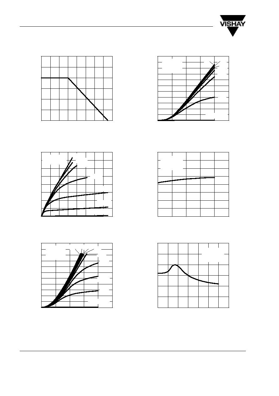
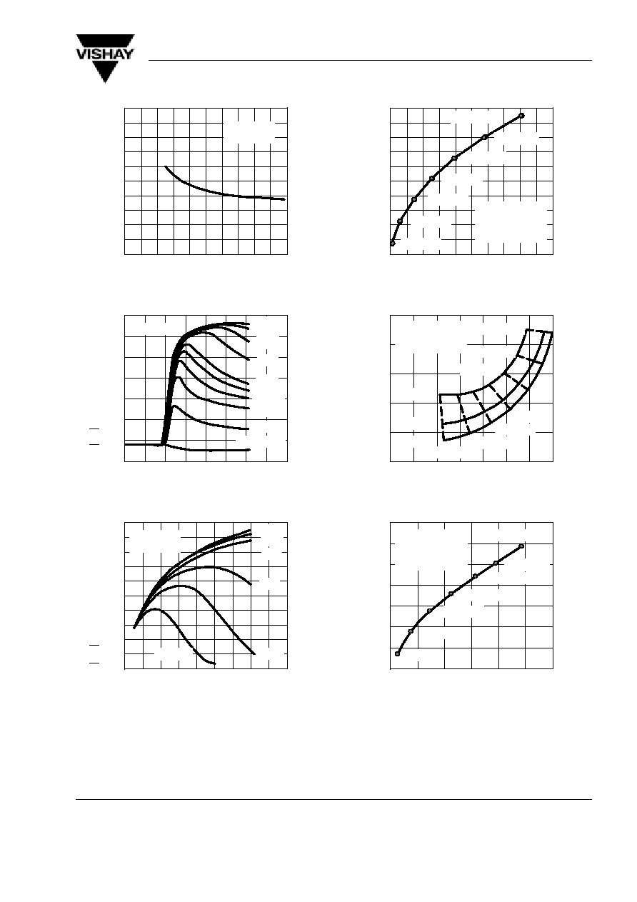
Figure 1. Total Power Dissipation vs.
Ambient Temperature
0
4
8
12
16
20
24
28
32
0
2
4
6
8
10
12
14
16
V
DS
Drain Source Voltage ( V )
12849
I Drain Current ( mA
)
D
V
G1S
= 1V
1V
0
2V
0.5V
V
G2S
= 4V
P
tot
=200mW
0.5V
1.5V
Figure 2. Drain Current vs. Drain Source Voltage
0
2
4
6
8
10
12
14
16
18
20
22
1
0.5
0.0
0.5
1.0
1.5
V
G1S
Gate 1 Source Voltage ( V )
12851
I Drain Current ( mA
)
D
V
G2S
= 1V
5V 4V
0
2V
1V
3V
V
DS
= 15V
6V
0.5V
Figure 3. Drain Current vs. Gate 1 Source Voltage
0
2
4
6
8
10
12
14
16
18
20
22
1
0.5
0.0
0.5
1.0
1.5
V
G2S
Gate 2 Source Voltage ( V )
12852
I Drain Current ( mA
)
D
V
G1S
= 1V
0
2V
1V
3V
V
DS
= 15V
5V
4V
Figure 4. Drain Current vs. Gate 2 Source Voltage
0
0.5
1.0
1.5
2.0
2.5
3.0
3.5
4.0
1
0.5
0.0
0.5
1.0
1.5
I
D
Drain Current ( mA )
12853
C Gate 1 Input Capacitance ( pF )
issg1
V
DS
=15V
V
G2S
=4V
f=1MHz
Figure 5. Gate 1 Input Capacitance vs. Drain Current
0
0.5
1.0
1.5
2.0
2.5
3.0
2
1
0
1
2
3
4
5
V
G2S
Gate 2 Source Voltage ( V )
12854
C Gate 2 Input Capacitance ( pF )
issg2
V
DS
=15V
V
G1S
=0
f=1MHz
Figure 6. Gate 2 Input Capacitance vs.
Gate 2 Source Voltage
BF996S
Vishay Telefunken
www.vishay.de
·
FaxBack +1-408-970-5600
Rev. 3, 20-Jan-99
5 (8)
Document Number 85010
0
0.2
0.4
0.6
0.8
1.0
1.2
1.4
1.6
1.8
2.0
0
2
4
6
8
10 12 14 16 18 20
V
DS
Drain Source Voltage ( V )
12856
C Output Capacitance ( pF )
oss
V
G2S
=4V
f=1MHz
Figure 7. Output Capacitance vs. Drain Source Voltage
60
50
40
30
20
10
0
10
2.0 1.5 1.0 0.5 0.0
0.5
1.0
1.5
2.0
V
G1S
Gate 1 Source Voltage ( V )
12855
S
T
ransducer
Gain
(
dB
)
2
21
4V
0
2V
1V
3V
f= 200MHz
0.2V
V
G2S
=1V
0.8V
0.6V
0.4V
Figure 8. Transducer Gain vs. Gate 1 Source Voltage
0
2
4
6
8
10
12
14
16
18
20
0
2
4
6
8
10
12
14
16
18
I
D
Drain Current ( mA )
12850
V
DS
=15V
f=1MHz
4V
2V
3V
1V
0.5V
V
G2S
=0
y Forward
T
ransadmittance ( mS )
21s
Figure 9. Forward Transadmittance vs. Drain Current
0
2
4
6
8
10
12
14
16
18
20
0
1
2
3
4
5
6
7
8
9
10
Re (y
11
) ( mS )
12857
Im ( y ) ( mS )
11
V
DS
=15V
V
G2S
=4V
I
D
=10mA
f=100...1300MHz
700MHz
1100MHz
500MHz
900MHz
300MHz
f=1300MHz
100MHz
Figure 10. Short Circuit Input Admittance
25
20
15
10
5
0
15
10
5
0
5
10
15
20
Re (y
21
) ( mS )
12858
Im ( y ) ( mS )
21
V
DS
=15V
V
G2S
=4V
f=100...1300MHz
f=100MHz
1300MHz
500MHz
300MHz
1100MHz
900MHz
700MHz
I
D
=5mA
10mA
15mA
Figure 11. Short Circuit Forward Transfer Admittance
0
1
2
3
4
5
6
7
0.0
0.5
1.0
1.5
2.0
2.5
3.0
Re (y
22
) ( mS )
12859
Im ( y ) ( mS )
22
V
DS
=15V
V
G2S
=4V
I
D
=10mA
f=100...1300MHz
f=1300MHz
900MHz
500MHz
300MHz
100MHz
700MHz
1100MHz
Figure 12. Short Circuit Output Admittance