 | ÐлекÑÑоннÑй компоненÑ: BFR181TF | СкаÑаÑÑ:  PDF PDF  ZIP ZIP |
/home/web/doc/html/vishay/30346
BFR181TF
Document Number 85100
Rev. 1.3, 28-Apr-05
Vishay Semiconductors
www.vishay.com
1
2
1
3
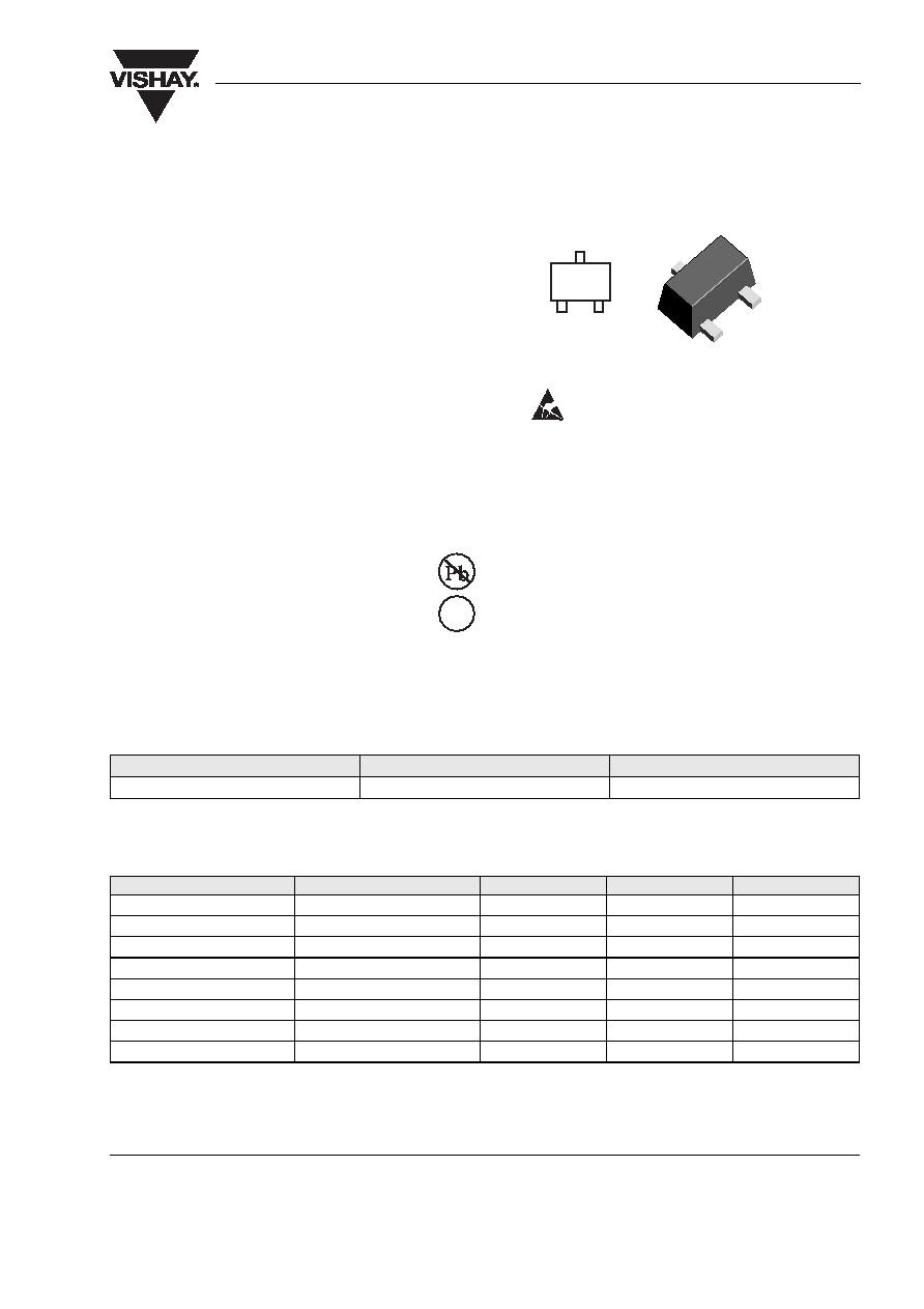
Electrostatic sensitive device.
Observe precautions for handling.
16867
Silicon NPN Planar RF Transistor
Description
The main purpose of this bipolar transistor is broad-
band amplification up to 2 GHz. In the space-saving
3-pin surface-mount SOT-490 package electrical per-
formance and reliability are taken to a new level cov-
ering a smaller footprint on PC boards than previous
packages. In addition to space savings, the SOT-490
provides a higher level of reliability than other 3-pin
packages, such as more resistance to moisture. Due
to the short length of its leads the SOT-490 is also
reducing package inductances resulting in some bet-
ter electrical performance. All of these aspects make
this device an ideal choice for demanding RF applica-
tions.
Features
· Small feedback capacitance
· Low noise figure
· High power gain
· Lead (Pb)-free component
· Component in accordance to RoHS 2002/95/EC
and WEEE 2002/96/EC
Applications
For low noise and high gain broadband amplifiers at
collector currents from 0.5 mA to 12 mA.
Mechanical Data
Typ: BFR181TF
Case: SOT-490 Plastic case
Weight: approx. 2.5 mg
Pinning: 1 = Collector, 2 = Base, 3 = Emitter
Parts Table
Absolute Maximum Ratings
T
amb
= 25 °C, unless otherwise specified
Part
Marking
Package
BFR181TF
RF
SOT-490
Parameter
Test condition
Symbol
Value
Unit
Collector-base voltage
V
CBO
15
V
Collector-emitter voltage
V
CEO
10
V
Emitter-base voltage
V
EBO
2
V
Collector current
I
C
20
mA
Base current
I
B
2
mA
Total power dissipation
T
amb
78 °C
P
tot
160
mW
Junction temperature
T
j
150
°C
Storage temperature range
T
stg
- 65 to + 150
°C
e3
www.vishay.com
2
Document Number 85100
Rev. 1.3, 28-Apr-05
BFR181TF
Vishay Semiconductors
Maximum Thermal Resistance
1)
on glass fibre printed board (25 x 20 x 1.5) mm
3
plated with 35
m Cu
Electrical DC Characteristics
T
amb
= 25 °C, unless otherwise specified
Parameter
Test condition
Symbol
Value
Unit
Junction ambient
1)
R
thJA
450
K/W
Parameter
Test condition
Symbol
Min
Typ.
Max
Unit
Collector-emitter cut-off current
V
CE
= 15 V, V
BE
= 0
I
CES
100
A
Collector-base cut-off current
V
CB
= 10 V, I
E
= 0
I
CBO
100
nA
Emitter-base cut-off current
V
EB
= 1 V, I
C
= 0
I
EBO
1
A
Collector-emitter breakdown
voltage
I
C
= 1 mA, I
B
= 0
V
(BR)CEO
10
V
Collector-emitter saturation
voltage
I
C
= 15 mA, I
B
= 1.5 mA
V
CEsat
0.1
0.4
V
DC forward current transfer ratio V
CE
= 6 V, I
C
= 5 mA
h
FE
50
100
V
CE
= 6 V, I
C
= 10 mA
h
FE
100
BFR181TF
Document Number 85100
Rev. 1.3, 28-Apr-05
Vishay Semiconductors
www.vishay.com
3
Electrical AC Characteristics
T
amb
= 25 °C, unless otherwise specified
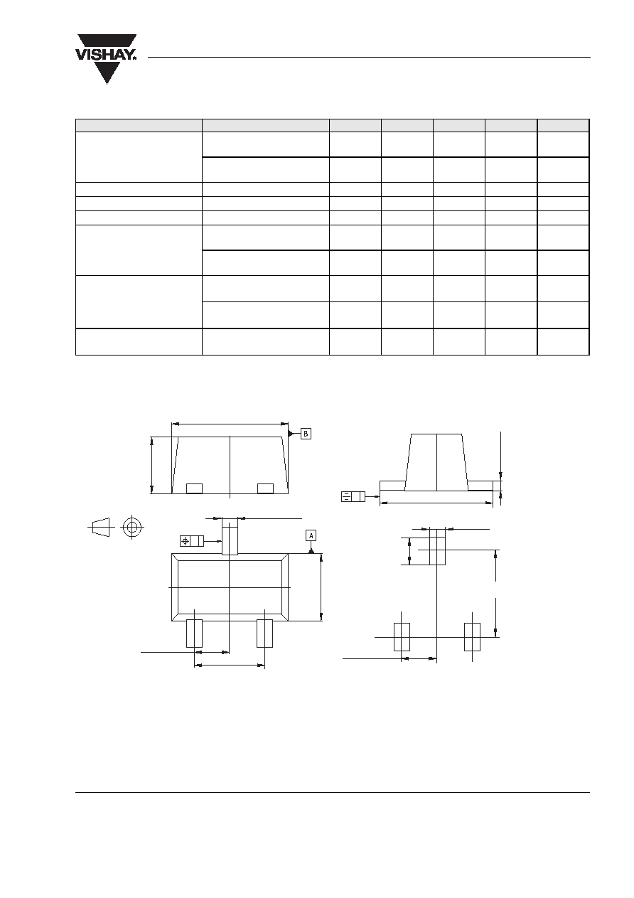
Package Dimensions in mm
Parameter
Test condition
Symbol
Min
Typ.
Max
Unit
Transition frequency
V
CE
= 3 V, I
C
= 6 mA,
f = 500 MHz
f
T
7
GHz
V
CE
= 8 V, I
C
= 20 mA,
f = 500 MHz
f
T
8
GHz
Collector-base capacitance
V
CB
= 10 V, f = 1 MHz
C
cb
0.3
pF
Collector-emitter capacitance
V
CE
= 10 V, f = 1 MHz
C
ce
0.2
pF
Emitter-base capacitance
V
EB
= 0.5 V, f = 1 MHz
C
eb
0.4
pF
Noise figure
V
CE
= 5 V, I
C
= 3 mA, Z
S
= Z
Sopt
,
f = 900 MHz
F
1.4
dB
V
CE
= 5 V, I
C
= 3 mA, Z
S
= Z
Sopt
,
f = 1.75 GHz
F
2.2
dB
Power gain
V
CE
= 8 V, Z
S
= 50
, Z
L
= Z
Lopt
,
I
C
= 8 mA, f = 900 MHz
G
pe
16
dB
V
CE
= 8 V, Z
S
= 50
, Z
L
= Z
Lopt
,
I
C
= 8 mA, f = 1.75 GHz
G
pe
12.5
dB
Transducer gain
V
CE
= 8 V, I
C
= 8 mA,
f = 900 MHz, Z
O
= 50
|S
21e
|
2
15
dB
16866
ISO Method E
0.4 (0.016)
0.5 (0.016)
0.65(0.026)
1.15(0.045)
0.1 B
0.1 A
1.5 (0.059)
1.7 (0.066)
0.6
(0.023)
0.8
(0.031)
3 x 0.20 (0.008)
3 x 0.30 (0.012)
1.5 (0.059)
1.7 (0.066)
0.75
(0.029)
0.95
(0.037)
0.10
(0.004)
0.20
(0.008)
0.5 (0.016)
1.0 (0.039)

www.vishay.com
4
Document Number 85100
Rev. 1.3, 28-Apr-05
BFR181TF
Vishay Semiconductors
Ozone Depleting Substances Policy Statement
It is the policy of Vishay Semiconductor GmbH to
1. Meet all present and future national and international statutory requirements.
2. Regularly and continuously improve the performance of our products, processes, distribution and operating
systems with respect to their impact on the health and safety of our employees and the public, as well as
their impact on the environment.
It is particular concern to control or eliminate releases of those substances into the atmosphere which are
known as ozone depleting substances (ODSs).
The Montreal Protocol (1987) and its London Amendments (1990) intend to severely restrict the use of ODSs
and forbid their use within the next ten years. Various national and international initiatives are pressing for an
earlier ban on these substances.
Vishay Semiconductor GmbH has been able to use its policy of continuous improvements to eliminate the use
of ODSs listed in the following documents.
1. Annex A, B and list of transitional substances of the Montreal Protocol and the London Amendments
respectively
2. Class I and II ozone depleting substances in the Clean Air Act Amendments of 1990 by the Environmental
Protection Agency (EPA) in the USA
3. Council Decision 88/540/EEC and 91/690/EEC Annex A, B and C (transitional substances) respectively.
Vishay Semiconductor GmbH can certify that our semiconductors are not manufactured with ozone depleting
substances and do not contain such substances.
We reserve the right to make changes to improve technical design
and may do so without further notice.
Parameters can vary in different applications. All operating parameters must be validated for each
customer application by the customer. Should the buyer use Vishay Semiconductors products for any
unintended or unauthorized application, the buyer shall indemnify Vishay Semiconductors against all
claims, costs, damages, and expenses, arising out of, directly or indirectly, any claim of personal
damage, injury or death associated with such unintended or unauthorized use.
Vishay Semiconductor GmbH, P.O.B. 3535, D-74025 Heilbronn, Germany

Legal Disclaimer Notice
Vishay
Document Number: 91000
www.vishay.com
Revision: 08-Apr-05
1
Notice
Specifications of the products displayed herein are subject to change without notice. Vishay Intertechnology, Inc.,
or anyone on its behalf, assumes no responsibility or liability for any errors or inaccuracies.
Information contained herein is intended to provide a product description only. No license, express or implied, by
estoppel or otherwise, to any intellectual property rights is granted by this document. Except as provided in Vishay's
terms and conditions of sale for such products, Vishay assumes no liability whatsoever, and disclaims any express
or implied warranty, relating to sale and/or use of Vishay products including liability or warranties relating to fitness
for a particular purpose, merchantability, or infringement of any patent, copyright, or other intellectual property right.
The products shown herein are not designed for use in medical, life-saving, or life-sustaining applications.
Customers using or selling these products for use in such applications do so at their own risk and agree to fully
indemnify Vishay for any damages resulting from such improper use or sale.
Document Outline