BFR92A/BFR92AR/BFR92AW
Vishay Telefunken
www.vishay.de
∑
FaxBack +1-408-970-5600
Rev. 3, 20-Jan-99
1 (10)
Document Number 85033
Silicon NPN Planar RF Transistor
Electrostatic sensitive device.
Observe precautions for handling.
Applications
Wide band amplifier up to GHz range.
Features
D
High power gain
D
Low noise figure
D
High transition frequency
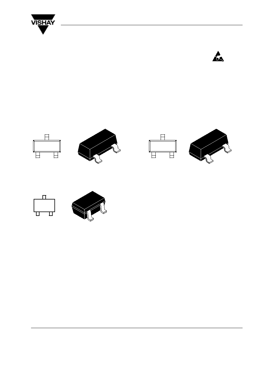
13 581
2
3
1
94 9280
BFR92A Marking: +P2
Plastic case (SOT 23)
1 = Collector, 2 = Base, 3 = Emitter
13 581
2
3
1
9510527
BFR92AR Marking: +P5
Plastic case (SOT 23)
1 = Collector, 2 = Base, 3 = Emitter
2
1
3
13 652
13 570
BFR92AW Marking: WP2
Plastic case (SOT 323)
1 = Collector, 2 = Base, 3 = Emitter
BFR92A/BFR92AR/BFR92AW
Vishay Telefunken
www.vishay.de
∑
FaxBack +1-408-970-5600
Rev. 3, 20-Jan-99
2 (10)
Document Number 85033
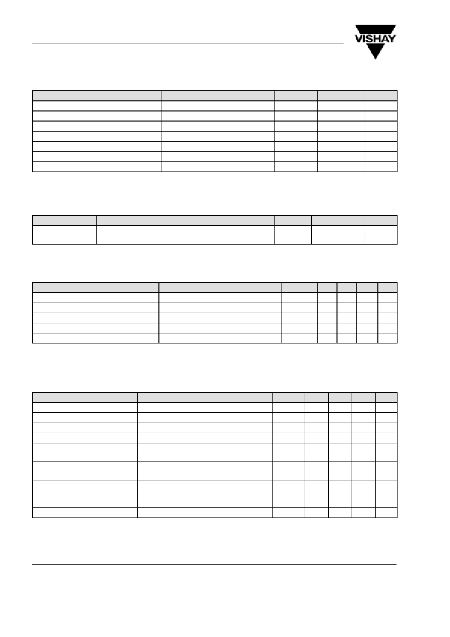
Absolute Maximum Ratings
T
amb
= 25
_
C, unless otherwise specified
Parameter
Test Conditions
Symbol
Value
Unit
Collector-base voltage
V
CBO
20
V
Collector-emitter voltage
V
CEO
15
V
Emitter-base voltage
V
EBO
2
V
Collector current
I
C
30
mA
Total power dissipation
T
amb
60
∞
C
P
tot
200
mW
Junction temperature
T
j
150
∞
C
Storage temperature range
T
stg
≠65 to +150
∞
C
Maximum Thermal Resistance
T
amb
= 25
_
C, unless otherwise specified
Parameter
Test Conditions
Symbol
Value
Unit
Junction ambient
on glass fibre printed board (25 x 20 x 1.5) mm
3
plated with 35
m
m Cu
R
thJA
450
K/W
Electrical DC Characteristics
T
amb
= 25
_
C, unless otherwise specified
Parameter
Test Conditions
Symbol
Min
Typ
Max Unit
Collector cut-off current
V
CE
= 20 V, V
BE
= 0
I
CES
100
m
A
Collector-base cut-off current
V
CB
= 10 V, I
E
= 0
I
CBO
100
nA
Emitter-base cut-off current
V
EB
= 2 V, I
C
= 0
I
EBO
10
m
A
Collector-emitter breakdown voltage I
C
= 1 mA, I
B
= 0
V
(BR)CEO
15
V
DC forward current transfer ratio
V
CE
= 10 V, I
C
= 14 mA
h
FE
65
100
150
Electrical AC Characteristics
T
amb
= 25
_
C, unless otherwise specified
Parameter
Test Conditions
Symbol
Min
Typ
Max
Unit
Transition frequency
V
CE
= 10 V, I
C
= 14 mA, f = 500 MHz
f
T
6
GHz
Collector-base capacitance
V
CB
= 10 V, f = 1 MHz
C
cb
0.3
pF
Collector-emitter capacitance
V
CE
= 10 V, f = 1 MHz
C
ce
0.15
pF
Emitter-base capacitance
V
EB
= 0.5 V, f = 1 MHz
C
eb
0.65
pF
Noise figure
V
CE
= 10 V, I
C
= 2 mA, Z
S
= 50
W
,
f = 800 MHz
F
1.8
dB
Power gain
V
CE
= 10 V, Z
S
= 50
W
, Z
L
= Z
Lopt
,
I
C
= 14 mA, f = 800 MHz
G
pe
16
dB
Linear output voltage ≠ two
tone intermodulation test
V
CE
= 10 V, I
C
= 14 mA, d
IM
= 60 dB,
f
1
= 806 MHz, f
2
= 810 MHz,
Z
S
= Z
L
= 50
W
V
1
= V
2
120
mV
Third order intercept point
V
CE
= 10 V, I
C
= 14 mA, f = 800 MHz
IP
3
24
dBm