VISHAY
BRT11/ 12/ 13
Document Number 83689
Rev. 1.4, 26-Apr-04
Vishay Semiconductors
www.vishay.com
1
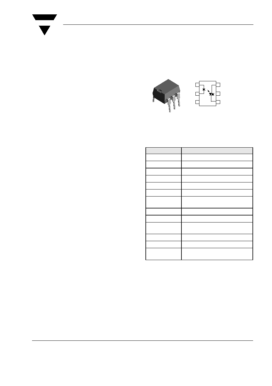
i179041
1
2
3
6
5
4
MT2
MT1
NC
A
C
NC
Optocoupler, Phototriac Output
Features
∑ I
TRMS
= 300 mA
∑ High Static dV
crq
/dt < 10,000 V/
µs
∑ Electrically Insulated between Input and output cir-
cuit
∑ Microcomputer compatible - Very Low Trigger
Current
∑ Non-zero voltage detectors High input Sensitivity
Agency Approvals
∑ UL - File No. E52744 System Code J
∑ DIN EN 60747-5-2(VDE0884)
DIN EN 60747-5-5 pending
Available with Option 1
Applications
Industrial controls
Office equipment
Consumer appliances
Description
The BRT11/12/13 are AC optocouplers non-zero volt-
age detectors consisting of two electrically insulated
lateral power ICs which integrate a thyristor system, a
photo detector and noise suppression at the output
and an IR GaAs diode input.
Order Information
For additional information on the available options refer to
Option Information.
Part
Remarks
BRT11-H
400 V V
DRM
, 2 mA I
FT
, DIP-6
BRT12-H
600 V V
DRM
, 2 mA I
FT
, DIP-6
BRT13-H
800 V V
DRM
, 2 mA I
FT
, DIP-6
BRT11-M
400 V V
DRM
, 3 mA I
FT
, DIP-6
BRT12-M
600 V V
DRM
, 3 mA I
FT
, DIP-6
BRT13-M
800 V V
DRM
, 3 mA I
FT
, DIP-6
BRT12-H-X006
600 V V
DRM
, 2 mA I
FT
, DIP-6 400 mil
(option 6)
BRT12-H-X007
600 V V
DRM
, 2 mA I
FT
, SMD-6 (option 7)
BRT12-H-X009
600 V V
DRM
, 2 mA I
FT
, SMD-6 (option 9)
BRT13-H-X006
800 V V
DRM
, 2 mA I
FT
, DIP-6 400 mil
(option 6)
BRT13-H-X007
800 V V
DRM
, 2 mA I
FT
, SMD-6 (option 7)
BRT13-H-X009
800 V V
DRM
, 2 mA I
FT
, SMD-6 (option 9)
BRT12-M-X006
600 V V
DRM
, 3 mA I
FT
, DIP-6 400 mil
(option 6)
www.vishay.com
2
Document Number 83689
Rev. 1.4, 26-Apr-04
VISHAY
BRT11/ 12/ 13
Vishay Semiconductors
Absolute Maximum Ratings
T
amb
= 25 ∞C, unless otherwise specified
Stresses in excess of the absolute Maximum Ratings can cause permanent damage to the device. Functional operation of the device is
not implied at these or any other conditions in excess of those given in the operational sections of this document. Exposure to absolute
Maximum Rating for extended periods of the time can adversely affect reliability.
Input
Output
Coupler
1)
Test AC voltage in acc. with DIN 57883, June 1980
Parameter
Test condition
Symbol
Value
Unit
Reverse voltage
V
R
6
V
Forward continuous current
I
F
20
mA
Surge forward current
I
FSM
1.5
A
Power dissipation
t
10 µs
P
diss
30
mW
Parameter
Test condition
Part
Symbol
Value
Unit
Repetitive peak off-state voltage
BRT11
V
DRM
400
V
BRT12
V
DRM
600
V
BRT13
V
DRM
800
V
RMS on-state current
I
TRMS
300
mA
Single cycle surge current
50 Hz
I
TSM
3
A
Power dissipation
P
diss
600
mW
Parameter
Test condition
Symbol
Value
Unit
Max. power dissipation
P
tot
630
mW
Ambient temperature
T
amb
- 40 to + 100
∞C
Storage temperature
T
stg
- 40 to + 150
∞C
Insulation test voltage
1)
between input/output circuit
(climate in acc. with DIN 40046,
part 2, Nov. 74)
V
ISO
5300
V
RMS
Reference voltage in acc. with
VDE 0110 b
V
ref
500
V
RMS
Reference voltage in acc. with
VDE 0110 b (insulation group C)
V
ref
600
V
DC
Creepage resistance (in acc.
with DIN IEC 112/VDE 0303,
part 1)
(group IIIa acc. to DIN VDE
0109)
CTI
175
Insulation resistance
V
IO
= 500 V, T
amb
= 25 ∞ C
R
IO
10
12
V
IO
= 500 V, T
amb
= 100 ∞ C
R
IO
10
11
DIN humidity category,
DIN 40 040
F
Creepage distance
(input/output circuit)
7.2
mm
Clearance (input/output circuit)
7.2
mm
VISHAY
BRT11/ 12/ 13
Document Number 83689
Rev. 1.4, 26-Apr-04
Vishay Semiconductors
www.vishay.com
3
Electrical Characteristics
T
amb
= 25 ∞C, unless otherwise specified
Minimum and maximum values are testing requirements. Typical values are characteristics of the device and are the result of engineering
evaluation. Typical values are for information only and are not part of the testing requirements.
Input
2)
Static air, SITAC soldered in pcb or base plate.
Output
2)
Static air, SITAC soldered in pcb or base plate.
Coupler
Parameter
Test condition
Symbol
Min
Typ.
Max
Unit
Forward voltage
I
F
= 10 mA
V
F
1.1
1.35
V
Reverse current
V
R
= 6 V
I
R
10
µA
Thermal resistance
2)
junction - ambient
R
thja
750
∞C/W
Parameter
Test condition
Symbol
Min
Typ.
Max
Unit
Critical rate of rise of off-state
voltage
V
D
= 0.67 V
DRM
, T
J
= 25 ∞C
dV/dt
cr
10
kV/
µs
V
D
= 0.67 V
DRM
, T
J
= 80 ∞C
dV/dt
cr
5
kV/
µs
Critical rate of rise of voltage at
current commutation
V
D
= 0.67 V
DRM
, T
J
= 25 ∞C,
dI/dt
crq
15 A/ms
dV/dt
crq
10
kV/
µs
V
D
= 0.67 V
DRM
, T
J
= 80 ∞C,
dI/dt
crq
15 A/ms
dV/dt
crq
5
kV/
µs
Critical rate of rise of on-state
current
dI/dt
cr
8
A/
µs
Pulse current
t
p
5 µs, f 0 100 Hz,
dI
tp
/dt
8 A/µs
I
tp
2
A
On-state voltage
I
T
= 300 mA
V
T
2.3
V
Off-state current
T
C
= 80 ∞C, V
DRM
I
D
0.5
100
µA
Holding current
V
D
= 10 V
I
H
80
500
µA
Thermal resistance
2)
junction -
ambient
R
thJA
R
thja
125
∞C/W
Parameter
Test condition
Symbol
Min
Typ.
Max
Unit
Trigger current
V
D
= 10 V, H - Versions
I
FT
0.4
2
mA
V
D
= 10 V, M - Versions
I
FT
0.8
3
mA
Trigger current temperature
gradient
I
FT
/
T
j
7
14
µA/∞C
Capacitance (input-output)
V
R
= 0 V, f = 1 kHz
C
IO
2
pF
www.vishay.com
4
Document Number 83689
Rev. 1.4, 26-Apr-04
VISHAY
BRT11/ 12/ 13
Vishay Semiconductors
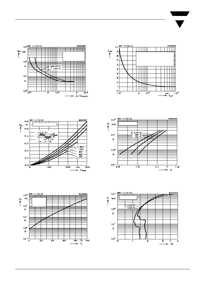
Typical Characteristics
(T
amb
= 25
∞C unless otherwise specified)
Fig. 1 Typical Trigger Delay Time
Fig. 2 Power Dissipation 40 to 60 Hz Line Operation
Fig. 3 Typical Off-State Current
17239
t
gd
=
f(I
F
/
I
FT25∞C
)
V
D
=200V
17240
P
tot= (
I
TRMS
)
17241
I
D
=
f(T
j
)
V
D
=800V
Fig. 4 Pulse Trigger Current
Fig. 5 Typical Input Characteristics
Fig. 6 Typical Output Characteristics
17242
IFTN=f(tpIF)
IFTN normalized to IFT refering
to tpIF
1 m
Vop=220V,f= 4 0 ...60Hz typ.
17243
I
F
= (
V
F
)
17244
I
T
= (
V
T
)
VISHAY
BRT11/ 12/ 13
Document Number 83689
Rev. 1.4, 26-Apr-04
Vishay Semiconductors
www.vishay.com
5
Package Dimensions in Inches (mm)
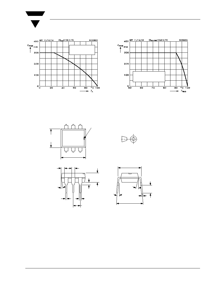
Fig. 7 Current Reduction
17245
ITRMS = (TA)
RthJA = 125 K/W 3)
Fig. 8 Current Reduction
17246
I
TRMS
= (
T
PIN5
)
RthJ-PIN5 = 16,5 K/W 4)
i178014
.008 (.20)
.012 (.30)
.130 (3.30)
.150 (3.81)
.130 (3.30)
.150 (3.81)
.033 (0.84) typ.
.300 (7.62)
typ.
.033 (0.84) typ.
.100 (2.54) typ
.039
(1.00)
Min.
.018 (0.46)
.020 (0.51)
.048 (1.22)
.052 (1.32)
.248 (6.30)
.256 (6.50)
.335 (8.50)
.343 (8.70)
pin one ID
6
5
4
1
2
3
18∞
3∞≠9∞
.300≠.347
(7.62≠8.81)
4∞
typ .
ISO Method A