BRT21/ 22/ 23
Document Number 83690
Rev. 1.4, 10-Jan-05
Vishay Semiconductors
www.vishay.com
1
17223
1
2
3
6
5
4
MT2
MT1
A
C
NC
*Zero Crossing Circuit
ZCC*
NC
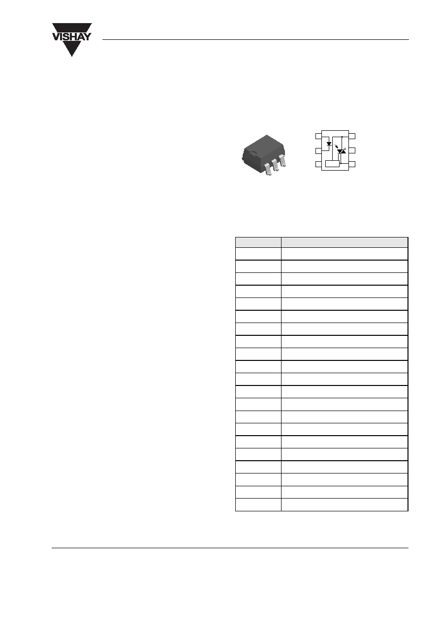
Optocoupler, Phototriac Output, Zero Crossing
Features
∑ High Input Sensitivity I
FT
= 1.0 mA
∑ I
TRMS
= 300 mA
∑ High Static dv/dt 10,000 V/
µs
∑ Electrically Insulated between Input and
Output circuit
∑ Microcomputer compatible
∑ Trigger Current
- (I
FT
< 1.2 mA) BRT22F, BRT23F,
- (I
FT
< 2 mA) BRT21H, BRT22H, BRT23H
- (I
FT
< 3 mA) BRT21M, BRT22M, BRT23M
∑ Available Surface Mount and on on tape and reel
∑ Zero Voltage Crossing detector
∑ UL File E52744 System Code "J"
∑ Lead-free component
∑ Component in accordance to RoHS 2002/95/EC
and WEEE 2002/96/EC
Applications
∑ Industrial controls
∑ Office equipment
∑ Consumer appliances
Description
The BRT21, BRT22, BRT23 product family consists
of AC switch optocouplers with zero voltage detec-
tors with two electrically insulated lateral power ICs
which integrate a thyrister system, a photo detector
and noise suppression at the output and an IR GaAs
diode input
High input sensitivity is achieved by using an emitter
follower phototransistor and an SCR predriver result-
ing in an LED trigger current of less than 2 mA or 3 mA
(DC). Inverse parallel SCRs provide commutating
dv/dt greater than 10 kV/
µs
The zero cross line voltage detection circuit consists
of two MOSFETS and a photodiode.
THe BRT21/ 22/ 23 product family isolates low-volt-
age logic from 120, 230 and 380 VAC lines to control
resistive, inductive or capacitive loads including
motors, solenoids, high current thyristers or TRIAC
and relays.
Order Information
For additional information on the available options refer to
Option Information.
Part
Remarks
BRT21H
V
DRM
400 V, DIP-6, 2.0 mA I
FT
BRT21M
V
DRM
400 V, DIP-6, 3.0 mA I
FT
BRT22F
V
DRM
600 V, DIP-6, 1.2 mA I
FT
BRT22H
V
DRM
600 V, DIP-6, 2.0 mA I
FT
BRT22M
V
DRM
600 V, DIP-6, 3.0 mA I
FT
BRT23F
V
DRM
800 V, DIP-6, 1.2 mA I
FT
BRT23H
V
DRM
800 V, DIP-6, 2.0 mA I
FT
BRT23M
V
DRM
800 V, DIP-6, 3.0 mA I
FT
BRT21H-X006
V
DRM
400 V, DIP-6 400 mil (option 6), 2.0 mA I
FT
BRT21H-X007
V
DRM
400 V, SMD-6 (option 7), 2.0 mA I
FT
BRT21M-X006
V
DRM
400 V, DIP-6 400 mil (option 6), 3.0 mA I
FT
BRT22F-X006
V
DRM
600 V, SMD-6 (option 7), 1.2 mA I
FT
BRT22F-X0067 V
DRM
600 V, SMD-6 (option 7), 1.2 mA I
FT
BRT22H-X007
V
DRM
600 V, SMD-6 (option 7), 2.0 mA I
FT
BRT22M-X006
V
DRM
600 V, DIP-6 400 mil (option 6), 3.0 mA I
FT
BRT23F-X006
V
DRM
800 V, DIP-6 400 mil (option 6), 1.2 mA I
FT
BRT23F-X007
V
DRM
800 V, DIP-6 400 mil (option 6), 1.2 mA I
FT
BRT23H-X006
V
DRM
800 V, DIP-6 400 mil (option 6), 2.0 mA I
FT
BRT23H-X007
V
DRM
800 V, SMD-6 (option 7), 2.0 mA I
FT
BRT23M-X006
V
DRM
800 V, DIP-6 400 mil (option 6), 3.0 mA I
FT
BRT23M-X007
V
DRM
800 V, SMD-6 (option 7), 3.0 mA I
FT
www.vishay.com
2
Document Number 83690
Rev. 1.4, 10-Jan-05
BRT21/ 22/ 23
Vishay Semiconductors
Absolute Maximum Ratings
T
amb
= 25 ∞C, unless otherwise specified
Stresses in excess of the absolute Maximum Ratings can cause permanent damage to the device. Functional operation of the device is
not implied at these or any other conditions in excess of those given in the operational sections of this document. Exposure to absolute
Maximum Rating for extended periods of the time can adversely affect reliability.
Input
Output
Coupler
Parameter
Test condition
Symbol
Value
Unit
Reverse voltage
I
R
= 10
µA
V
R
6.0
V
Forward current
I
F
60
mA
Surge current
I
FSM
2.5
A
Power dissipation
P
diss
100
mW
Derate from 25 ∞C
1.33
mW/∞C
Parameter
Test condition
Part
Symbol
Value
Unit
Peak off-state voltage
I
D(RMS)
= 70
µA
BRT21
V
DM
400
V
BRT22
V
DM
600
V
BRT23
V
DM
800
V
RMS on-state current
I
TM
300
mA
Single cycle surge current
3.0
A
Power dissipation
P
diss
600
mW
Derate from 25 ∞C
6.6
mW/∞C
Parameter
Test condition
Symbol
Value
Unit
Isolation test voltage (between
emitter and detector, climate per
DIN 500414, part 2, Nov. 74)
t = 1.0 min.
V
ISO
5300
V
RMS
Pollution degree (DIN VDE
0109)
2
Creepage
7.0
mm
Clearance
7.0
mm
Comparative tracking index per
DIN IEC 112/VDE 0303 part 1,
group IIIa per DIN VDE 6110
175
Isolation resistance
V
IO
= 500 V, T
amb
= 25 ∞C
R
IO
10
12
V
IO
= 500 V, T
amb
= 100 ∞C
R
IO
10
11
Storage temperature range
T
stg
- 55 to + 150
∞C
Ambient temperature range
T
amb
- 55 to + 100
∞C
Soldering temperature
max.
10 sec. dip soldering
0.5 mm from case bottom
T
sld
260
∞C
BRT21/ 22/ 23
Document Number 83690
Rev. 1.4, 10-Jan-05
Vishay Semiconductors
www.vishay.com
3
Electrical Characteristics
T
amb
= 25 ∞C, unless otherwise specified
Minimum and maximum values are testing requirements. Typical values are characteristics of the device and are the result of engineering
evaluation. Typical values are for information only and are not part of the testing requirements.
Input
Output
Parameter
Test condition
Symbol
Min
Typ.
Max
Unit
Forward voltage
I
F
= 10 mA
V
F
1.16
1.35
V
Reverse current
V
R
= 6.0 V
I
R
0.1
10
µA
Capacitance
V
F
= 0 V, f = 1.0 MHz
C
O
25
pF
Thermal resistance, junction to
ambient
R
thja
750
K/W
Parameter
Test condition
Symbol
Min
Typ.
Max
Unit
Off-state voltage
I
D(RMS)
= 70
µA
V
D(RMS)
424
460
V
Repetitive peak off-state voltage I
DRM
= 100
µA
V
DRM
600
V
Off-state current
V
D
= V
DRM
, T
amb
= 100 ∞C,
I
F
= 0 mA
I
D(RMS)
10
100
µA
On-state voltage
I
T
= 300 mA
V
TM
1.7
3.0
V
On-state current
PF = 1.0, V
T(RMS)
= 1.7 V
I
TM
300
mA
Surge (non-repetitive), on-state
current
f = 50 Hz
I
TSM
3.0
A
Trigger current temp. gradient
I
FT1
/
T
j
7.0
14
µA/K
I
FT2
/
T
j
7.0
14
µA/K
Inhibit voltage temp. gradient
V
DINH
/
T
j
-20
mV/K
Off-state current in inhibit state
I
F
= I
FT1
, V
DRM
I
DINH
50
200
µA
Holding current
I
H
65
500
µA
Latching current
V
T
= 2.2 V
I
L
5.0
mA
Zero cross inhibit voltage
I
F
= Rated I
FT
V
IH
15
25
V
Turn-on time
V
RM
= V
DM
= V
D(RMS)
t
on
35
µs
Turn-off time
PF = 1.0, I
T
= 300 mA
t
off
50
µs
Critical rate of rise of off-state
voltage
V
D
= 0.67 V
DRM
, T
J
= 25 ∞C
dv/dt
cr
10000
V/
µs
V
D
= 0.67 V
DRM
, T
J
= 80 ∞C
dv/dt
cr
5000
V/
µs
Critical rate of rise of voltage at
current commutation
V
D
= 0.67 V
DRM
,
di/dt
crq
15 A/ms, T
j
= 25 ∞C
dv/dt
crq
10000
V/
µs
V
D
= 0.67 V
DRM
,
di/dt
crq
15 A/ms, T
j
= 80 ∞C
dv/dt
crq
5000
V/
µs
Critical rate of rise of on-state
di/dt
cr
8.0
A/
µs
Thermal resistance, junction to
ambient
R
thja
125
K/W
www.vishay.com
4
Document Number 83690
Rev. 1.4, 10-Jan-05
BRT21/ 22/ 23
Vishay Semiconductors
Coupler
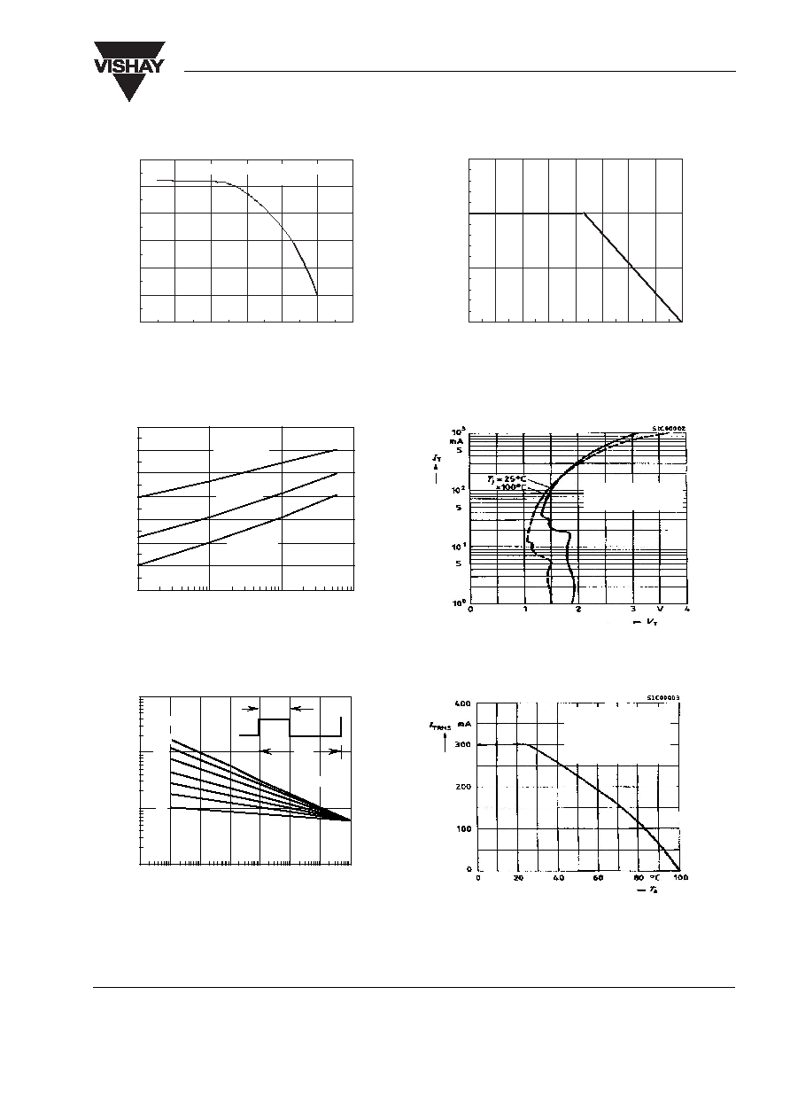
Power Factor Considerations
A snubber isn't needed to eliminate false operation of
the TRIAC driver because of the high static and com-
mutating dv/dt with loads between 1.0 and 0.8 power
factors. When inductive loads with power factors less
than 0.8 are being driven, include a RC snubber or a
single capacitor directly across the device to damp
the peak commutating dv/ dt spike. Normally a com-
mutating dv/dt causes a turning-off device to stay on
due to the stored energy remaining in the turning-off
device.
But in the case of a zero voltage crossing optotriac,
the commutating dv/dt spikes can inhibit one half of
the TRIAC from turning on. If the spike potential
exceeds the inhibit voltage of the zero cross detection
circuit, half of the TRIAC will be heldoff and not turn-
on. This hold-off condition can be eliminated by using
a snubber or capacitor placed directly across the
optotriac as shown in Figure 1. Note that the value of
the capacitor increases as a function of the load cur-
rent.
The hold-off condition also can be eliminated by pro-
viding a higher level of LED drive current. The higher
LED drive provides a larger photocurrent which
causes the phototransistor to turn-on before the com-
mutating spike has activated the zero cross network.
Figure 2 shows the relationship of the LED drive for
power factors of less than 1.0. The curve shows that
if a device requires 1.5 mA for a resistive load, then
1.8 times 2.7 mA) that amount would be required to
control an inductive load whose power factor is less
than 0.3.
Parameter
Test condition
Symbol
Min
Typ.
Max
Unit
Critical rate of rise of coupled
input/output voltage
I
T
= 0 A, V
RM
= V
DM
= V
D(RMS)
dv
IO
/dt
10000
V/
µs
Common mode coupling
capacitance
C
CM
0.01
pF
Capacitance (input-output)
f = 1.0 MHz, V
IO
= 0 V
C
IO
0.8
pF
Isolation resistance
V
IO
= 500 V, T
amb
= 25 ∞C
R
is
10
12
V
IO
= 500 V, T
amb
= 100 ∞C
R
is
10
11
Trigger current
V
D
= 5.0 V, F - Versions
I
FT
1.2
mA
V
D
= 5.0 V, H - Versions
I
FT
2.0
mA
V
D
= 5.0 V, M - Versions
I
FT
3.0
mA
Figure 1. Shunt Capacitance vs. Load Current
iil410_01
400
350
300
250
200
150
100
50
0
.001
.01
.1
1
IL - Load Current - mA(RMS)
Cs
-
Shunt
C
apacitance
-
µ
F
Cs(
µF) = 0.0032 (µF)* 10^(0.0066IL (mA)
Ta = 25∞C, PF = 0.3
IF = 2.0 mA
BRT21/ 22/ 23
Document Number 83690
Rev. 1.4, 10-Jan-05
Vishay Semiconductors
www.vishay.com
5
Typical Characteristics (Tamb = 25
∞C unless otherwise specified)
Figure 2. Normalized LED Trigger Current vs. Power Factor
Figure 3. Forward Voltage vs. Forward Current
Figure 4. Peak LED Current vs. Duty Factor, Tau
iil410_02
1.2
1.0
0.8
0.6
0.4
0.2
0.0
0.8
1.0
1.2
1.4
1.6
1.8
2.0
PF - Power Factor
NIFth
-
Normalized
LED
Trigger
Current
Ta = 25∞C
IFth Normalized to IFth @ PF = 1.0
iil410_03
100
10
1
.1
0.7
0.8
0.9
1.0
1.1
1.2
1.3
1.4
IF - Forward Current - mA
VF
-
Forward
Voltage
-
V
Ta = -55∞C
Ta = 25∞C
Ta = 85∞C
iil410_04
10-6
10-5
10-4
10 -3
10-2
10-1
10 0
101
10
100
1000
10000
t -LED Pulse Duration -s
If(pk)
-
Peak
LED
Current
-
m
A
.005
.05
.02
.01
.1
.2
.5
Duty Factor
t
DF = /t
Figure 5. Maximum LED Power Dissipation
Figure 6. Typical Output Characteristics
Figure 7. Current Reduction
iil410_05
100
80
60
40
20
0
-20
-40
-60
0
50
100
150
Ta - Ambient Temperature - ∞C
LED
-
LED
Power
-
m
W
iil410_06
IT = f(VT),
parameter: Tj
iil410_07
I
TRMS
=f(T
A
),
R
thJA
=150 K/W
Device switch
soldered in pcb
or base plate.
www.vishay.com
6
Document Number 83690
Rev. 1.4, 10-Jan-05
BRT21/ 22/ 23
Vishay Semiconductors
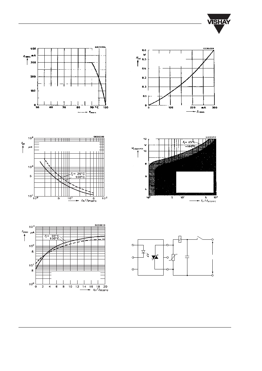
Figure 8. Current Reduction
Figure 9. Typical Trigger Delay Time
Figure 10. Typical Inhibit Current
iil410_08
I
TRMS
=f(T
PIN5
), R
thJ≠PIN5
=16.5 K/W
Thermocouple measurement must
be performed potentially separated
to A1 and A2. Measuring junction
as near as possible at the case.
iil410_09
t
gd
=f (I
F
I
FT
25∞C), V
D
=200 V,
f=40 to 60 Hz, parameter: T
j
iil410_10
I
DINH
=f (I
F
/I
FT
25∞C),
V
D
=600 V, parameter: T
j
Figure 11. Power Dissipation 40 to 60 Hz Line Operation
Figure 12. Typical Static Inhibit Voltage Limit
Figure 13. 1- Apply a Capacitor to the Supply Pins at the Load-Side
40 to 60 Hz
line operation,
P
tot
=f(I
TRMS
)
iil410_11
iil410_12
V
DINHmin
=f(I
F
/I
FT
25∞C),
parameter: T
j
Device zero voltage
switch can be triggered
only in hatched area
below Tj curves.
iil410_13
0.1
µF
220 V~
1
2
3
6
5
4
BRT21/ 22/ 23
Document Number 83690
Rev. 1.4, 10-Jan-05
Vishay Semiconductors
www.vishay.com
7
Technical Information
See Application Note for additional information.
Package Dimensions in Inches (mm)
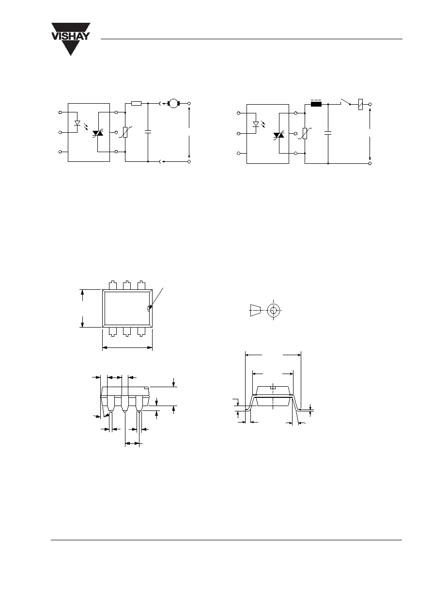
Figure 14. 2 - Connect a Series Resistor to the Output and Bridge
Both by a Capacitor
iil410_14
22 nF
220 V~
2
1
3
5
6
4
33
Figure 15. 3 - Connect a Choke of Low Winding Cap. in Series,
e.g., a Ringcore Choke, with Higher Load Currents
iil410_15
22 nF
220 V~
1
2
3
5
4
6
500
µH
.020 (.51)
.040 (1.02)
.300 (7.62)
ref.
.375 (9.53)
.395 (10.03)
.012 (.30) typ.
.0040 (.102)
.0098 (.249)
15i max.
.248 (6.30)
.256 (6.50)
.335 (8.50)
.343 (8.70)
pin one ID
6
5
4
1
2
3
ISO Method A
.130 (3.30)
.150 (3.81)
.033 (0.84) typ.
.033 (0.84) typ.
.100 (2.54) typ
.039
(1.00)
Min.
.018 (0.46)
.020 (0.51)
.048 (1.22)
.052 (1.32)
4∞
typ .
17222
www.vishay.com
8
Document Number 83690
Rev. 1.4, 10-Jan-05
BRT21/ 22/ 23
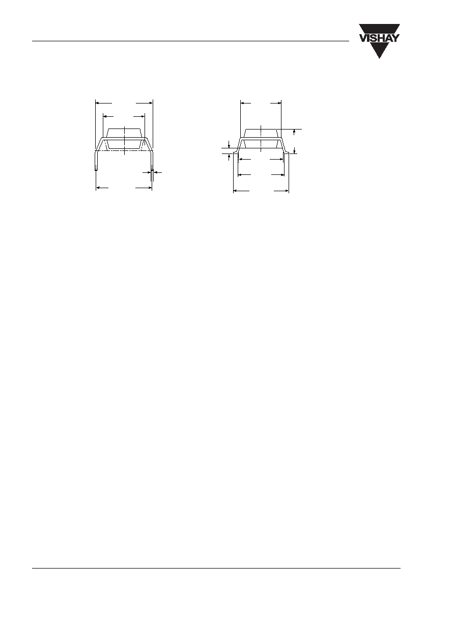
Vishay Semiconductors
.014 (0.35)
.010 (0.25)
.400 (10.16)
.430 (10.92)
.307 (7.8)
.291 (7.4)
.407 (10.36)
.391 (9.96)
Option 6
.315 (8.0)
MIN.
.300 (7.62)
TYP.
.180 (4.6)
.160 (4.1)
.331 (8.4)
MIN.
.406 (10.3)
MAX.
.028 (0.7)
MIN.
Option 7
18487

BRT21/ 22/ 23
Document Number 83690
Rev. 1.4, 10-Jan-05
Vishay Semiconductors
www.vishay.com
9
Ozone Depleting Substances Policy Statement
It is the policy of Vishay Semiconductor GmbH to
1. Meet all present and future national and international statutory requirements.
2. Regularly and continuously improve the performance of our products, processes, distribution and
operatingsystems with respect to their impact on the health and safety of our employees and the public, as
well as their impact on the environment.
It is particular concern to control or eliminate releases of those substances into the atmosphere which are
known as ozone depleting substances (ODSs).
The Montreal Protocol (1987) and its London Amendments (1990) intend to severely restrict the use of ODSs
and forbid their use within the next ten years. Various national and international initiatives are pressing for an
earlier ban on these substances.
Vishay Semiconductor GmbH has been able to use its policy of continuous improvements to eliminate the use
of ODSs listed in the following documents.
1. Annex A, B and list of transitional substances of the Montreal Protocol and the London Amendments
respectively
2. Class I and II ozone depleting substances in the Clean Air Act Amendments of 1990 by the Environmental
Protection Agency (EPA) in the USA
3. Council Decision 88/540/EEC and 91/690/EEC Annex A, B and C (transitional substances) respectively.
Vishay Semiconductor GmbH can certify that our semiconductors are not manufactured with ozone depleting
substances and do not contain such substances.
We reserve the right to make changes to improve technical design
and may do so without further notice.
Parameters can vary in different applications. All operating parameters must be validated for each
customer application by the customer. Should the buyer use Vishay Semiconductors products for any
unintended or unauthorized application, the buyer shall indemnify Vishay Semiconductors against all
claims, costs, damages, and expenses, arising out of, directly or indirectly, any claim of personal
damage, injury or death associated with such unintended or unauthorized use.
Vishay Semiconductor GmbH, P.O.B. 3535, D-74025 Heilbronn, Germany
Telephone: 49 (0)7131 67 2831, Fax number: 49 (0)7131 67 2423