 | ÐлекÑÑоннÑй компоненÑ: BS250KL | СкаÑаÑÑ:  PDF PDF  ZIP ZIP |
Äîêóìåíòàöèÿ è îïèñàíèÿ www.docs.chipfind.ru
FEATURES
D TrenchFETr Power MOSFET
D ESD Protected: 2000 V
APPLICATIONS
D Drivers: Relays, Solenoids, Lamps, Hammers,
Displays, Memories, Transistors, etc.
D Battery Operated Systems
D Power Supply, Converter Circuits
D Motor Control
TP0610KL/BS250KL
Vishay Siliconix
New Product
Document Number: 72712
S-40244--Rev. A, 16-Feb-04
www.vishay.com
1
P-Channel 60-V (D-S) MOSFET
PRODUCT SUMMARY
V
(BR)DSS(min)
(V)
r
DS(on)
(W)
V
GS(th)
(V)
I
D
(A)
60
6 @ V
GS
= -10 V
1 to 3 0
-0.27
-60
10 @ V
GS
= -4.5 V
-1 to -3.0
-0.21
Ordering Information: TP0610KL-TR1
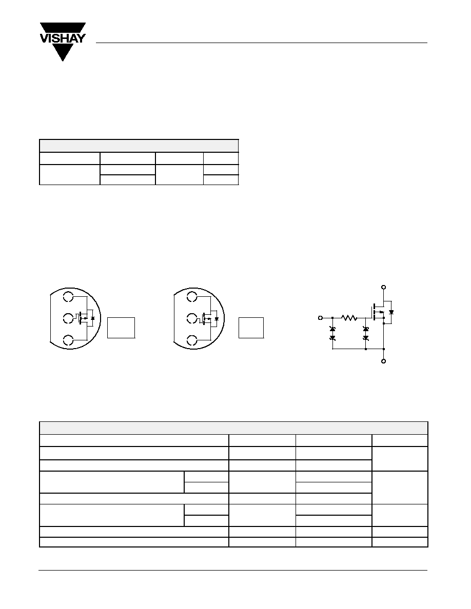
1
TO-226AA
(TO-92)
Top View
S
D
G
2
3
TO-92-18RM
(TO-18 Lead Form)
Top View
D
S
G
1
2
3
"S" TP
0610KL
xxyy
Device Marking
Front View
"S" = Siliconix Logo
xxyy = Date Code
Device Marking
Front View
"S" BS
250KL
xxyy
"S" = Siliconix Logo
xxyy = Date Code
D
S
G
100 W
Ordering Information: BS250KL-TR1
ABSOLUTE MAXIMUM RATINGS (T
A
= 25_C UNLESS OTHERWISE NOTED)
Parameter
Symbol
Limit
Unit
Drain-Source Voltage
V
DS
-60
V
Gate-Source Voltage
V
GS
"20
V
Continuous Drain Current
T
A
= 25_C
I
D
-0.27
Continuous Drain Current
T
A
= 70_C
I
D
-0.22
A
Pulse Drain Current
a
I
DM
-1.0
Power Dissipation
T
A
= 25_C
P
D
0.8
W
Power Dissipation
T
A
= 70_C
P
D
0.51
W
Maximum Junction-to-Ambient
R
thJA
156
_C/W
Operating Junction and Storage Temperature Range
T
J
, T
stg
-55 to 150
_C
Notes
a.
Pulse width limited by maximum junction temperature.
TP0610KL/BS250KL
Vishay Siliconix
New Product
www.vishay.com
2
Document Number: 72712
S-40244--Rev. A, 16-Feb-04
SPECIFICATIONS (T
A
= 25_C UNLESS OTHERWISE NOTED)
Parameter
Symbol
Test Condition
Min
Typ
Max
Unit
Static
Drain-Source Breakdown Voltage
V
(BR)DSS
V
GS
= 0 V, I
D
= -10 µA
-60
V
Gate-Threshold Voltage
V
GS(th)
V
DS
= V
GS
, I
D
= -250 µA
-1
-2.1
-3.0
V
V
DS
= 0 V, V
GS
= "20 V
"10
mA
Gate Body Leakage
I
GSS
V
DS
= 0 V, V
GS
= "10 V
"200
Gate-Body Leakage
I
GSS
V
DS
= 0 V, V
GS
= "10 V, T
J
= 85_C
"500
nA
V
DS
= 0 V, V
GS
= "5 V
"100
Zero Gate Voltage Drain Current
I
DSS
V
DS
= -60 V, V
GS
= 0 V
-1
mA
Zero Gate Voltage Drain Current
I
DSS
V
DS
= -60 V, V
GS
= 0 V, T
J
= 55_C
-10
mA
On State Drain Current
a
I
D( )
V
DS
= -10 V, V
GS
= -4.5 V
-50
mA
On-State Drain Current
a
I
D(on)
V
DS
= -10 V, V
GS
= -10 V
-600
mA
V
GS
= -4.5 V, I
D
= -25 mA
5.5
10
Drain-Source On-Resistance
a
r
DS(on)
V
GS
= -10 V, I
D
= -500 mA
3.1
6
W
DS(on)
V
GS
= -10 V, I
D
= -500 mA, T
J
= 125_C
4.7
9
Forward Transconductance
a
g
fs
V
DS
= -10 V, I
D
= -100 mA
180
mS
Diode Forward Voltage
a
V
SD
I
S
= -200 mA, V
GS
= 0 V
-0.9
-1.4
V
Dynamic
b
Total Gate Charge
Q
g
1.7
3
Gate-Source Charge
Q
gs
V
DS
= -30 V, V
GS
= -15 V, I
D
^ -500 mA
0.26
nC
Gate-Drain Charge
Q
gd
DS
GS
D
0.46
Gate Resistance
R
g
285
W
Turn On Time
t
d(on)
2.4
5
Turn-On Time
t
r
V
DD
= -25 V, R
L
= 150 W
I
D
^ -150 mA V
GEN
= -10 V
15.5
25
ns
Turn Off Time
t
d(off)
I
D
^ -150 mA, V
GEN
= -10 V
R
g
= 10 W
21
35
ns
Turn-Off Time
t
f
R
g
10 W
12.5
20
Notes
a.
Pulse test: PW v300 ms duty cycle v2%.
b.
Guaranteed by design, not subject to production testing.
TYPICAL CHARACTERISTICS (25_C UNLESS NOTED)
0
300
600
900
1200
0
2
4
6
8
10
0.0
0.2
0.4
0.6
0.8
1.0
0
1
2
3
4
5
Output Characteristics
Transfer Characteristics
V
DS
- Drain-to-Source Voltage (V)
-
Drain Current (A)
I D
V
GS
= 10 V
5 V
4 V
V
GS
- Gate-to-Source Voltage (V)
-
Drain Current (mA)
I D
T
J
= -55_C
125_C
25_C
6 V
7 V
8 V
For the following graphs, p-channel negative polarities for all voltage and current values are represented as positive values.
TP0610KL/BS250KL
Vishay Siliconix
New Product
Document Number: 72712
S-40244--Rev. A, 16-Feb-04
www.vishay.com
3
TYPICAL CHARACTERISTICS (25_C UNLESS NOTED)
0.0
0.3
0.6
0.9
1.2
1.5
1.8
-50
-25
0
25
50
75
100
125
150
On-Resistance vs. Junction Temperature
T
J
- Junction Temperature (_C)
V
GS
= 10 V @ 500 mA
V
GS
= 4.5 V @ 25 mA
0
3
6
9
12
15
0.0
0.3
0.6
0.9
1.2
1.5
1.8
I
D
= 500 mA
Gate Charge
-
Gate-to-Source V
oltage (V)
Q
g
- Total Gate Charge (nC)
V
GS
0
4
8
12
16
20
0
200
400
600
800
1000
On-Resistance vs. Drain Current
I
D
- Drain Current (mA)
V
GS
= 4.5 V
V
GS
= 10 V
-
On-Resistance (
r DS(on)
W
)
0
8
16
24
32
40
0
5
10
15
20
25
Capacitance
V
DS
- Drain-to-Source Voltage (V)
C
-
Capacitance (pF)
C
rss
C
oss
C
iss
V
GS
= 0 V
V
GS
= 5 V
V
DS
= 30 V
V
DS
= 48 V
For the following graphs, p-channel negative polarities for all voltage and current values are represented as positive values.
0
2
4
6
8
10
0
2
4
6
8
10
On-Resistance vs. Gate-Source Voltage
V
GS
- Gate-to-Source Voltage (V)
I
D
= 500 mA
I
D
= 200 mA
-
On-Resistance (
r DS(on)
W
)
1.2
1.5
1
100
1000
0.00
0.3
0.6
0.9
T
J
= 25_C
T
J
= 125_C
Source-Drain Diode Forward Voltage
V
SD
- Source-to-Drain Voltage (V)
-
Source Current (A)
I
S
10
T
J
= -55_C
V
GS
= 0 V
r
DS
(
on)
-
On-Resiistance
(Normalized)
TP0610KL/BS250KL
Vishay Siliconix
New Product
www.vishay.com
4
Document Number: 72712
S-40244--Rev. A, 16-Feb-04
TYPICAL CHARACTERISTICS (25_C UNLESS NOTED)
Threshold Voltage Variance Over Temperature
V
ariance (V)
V
GS(th)
-0.3
-0.2
-0.1
-0.0
0.1
0.2
0.3
0.4
0.5
-50
-25
0
25
50
75
100
125
150
I
D
= 250 mA
T
J
- Junction Temperature (_C)
10
-3
10
-2
1
10
600
10
-1
10
-4
100
2
1
0.1
0.01
0.2
0.1
0.05
0.02
Single Pulse
Duty Cycle = 0.5
Normalized Thermal Transient Impedance, Junction-to-Ambient
Square Wave Pulse Duration (sec)
Normalized Ef
fective
T
ransient
Thermal Impedance
1. Duty Cycle, D =
2. Per Unit Base = R
thJA
= 156_C/W
3. T
JM
- T
A
= P
DM
Z
thJA(t)
t
1
t
2
t
1
t
2
Notes:
4. Surface Mounted
P
DM
0.01
0
1
16
20
100
600
0.1
Power (W)
Single Pulse Power, Junction-to-Ambient
Time (sec)
12
4
8
10
For the following graphs, p-channel negative polarities for all voltage and current values are represented as positive values.
Safe Operating Area
V
DS
- Drain-to-Source Voltage (V)
10
0.1
0.1
1
10
100
0.001
1
T
A
= 25_C
Single Pulse
-
Drain Current (A)
I
D
0.01
I
DM
Limited
I
D(on)
Limited
r
DS(on)
Limited
BV
DSS
Limited
1 ms
10 ms
100 ms
dc
10 s
1 s