BZD27C3V6P to BZD27C200P
Document Number 85810
Rev. 1.8, 13-Apr-05
Vishay Semiconductors
www.vishay.com
1
17249
Zener Diodes with Surge Current Specification
Features
∑ Sillicon Planar Zener Diodes
∑ Low profile surface-mount package
∑ Zener and surge current specification
∑ Low leakage current
∑ Excellent stability
∑ High temperature soldering:
260 ∞C/10 sec. at terminals
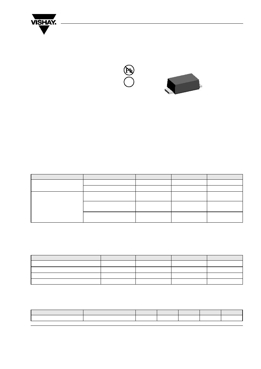
∑ Lead (Pb)-free component
∑ Component in accordance to RoHS 2002/95/EC
and WEEE 2002/96/EC
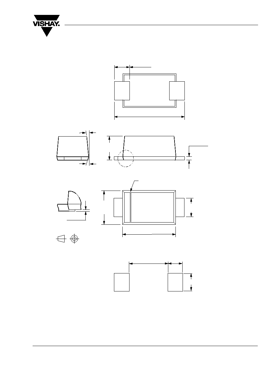
Mechanical Data
Case: JEDEC DO-219AB (SMF
Æ
) Plastic case
Weight: approx. 15 mg
Packaging codes/options:
GS18 / 10 k per 13 " reel, (8 mm tape), 50 k/box
GS08 / 3 k per 7 " reel, (8 mm tape), 30 k/box
Absolute Maximum Ratings
T
amb
= 25 ∞C, unless otherwise specified
1)
Mounted on epoxy-glass PCB with 3 x 3 mm Cu pads (
40 µm thick)
2)
T
J
= 25 ∞C prior to surge
Thermal Characteristics
T
amb
= 25 ∞C, unless otherwise specified
1)
Mounted on epoxy-glass PCB with 3 x 3 mm Cu pads (
40 µm thick)
Electrical Characteristics
T
amb
= 25 ∞C, unless otherwise specified
Parameter
Test condition
Symbol
Value
Unit
Power dissipation
T
L
= 80 ∞C
P
tot
2.3
W
T
A
= 25 ∞C
P
tot
0.8
1)
W
Non-repetitive peak pulse power
dissipation
100
µs square pulse
2)
P
ZSM
300
W
10/1000
µs waveform (BZD27-
C7V5P to BZD27-C100P)
2)
P
RSM
150
W
10/1000
µs waveform (BZD27-
C110P to BZD27-C200P)
2)
P
RSM
100
W
Parameter
Test condition
Symbol
Value
Unit
Thermal resistance junction to ambient air
1)
R
thJA
180
K/W
Thermal resistance junction to lead
R
thJL
30
K/W
Maximum junction temperature
T
j
150
∞C
Storage temperature range
T
S
- 55 to + 150
∞C
Parameter
Test condition
Symbol
Min
Typ.
Max
Unit
Forward voltage
I
F
= 0.2 A
V
F
1.2
V
e3

BZD27C3V6P to BZD27C200P
Document Number 85810
Rev. 1.8, 13-Apr-05
Vishay Semiconductors
www.vishay.com
3
Electrical Characteristics
When used as protection diodes (T
J
= 25 ∞C unless otherwise noted)
1)
Non-repetitive peak reverse current in accordance with "IEC 60-1, Section 8" (10/1000
µs pulse); see Fig. 5.
Partnumber
Rev.
Breakdown
Voltage
Test
Current
Temperature Coefficient
Clamping Voltage
Reverse Current at
Stand-Off Voltage
V
(BR)R
at
I
test
I
test
Z
@ I
test
V
C
at I
RSM
1)
I
R
at V
WM
V
mA
%/∞C
V
A
µA
V
min
min
max
max
max
BZD27C7V5P
7
100
0
0.07
11.3
13.3
1500
6.2
BZD27C8V2P
7.7
100
0.03
0.08
12.3
12.2
1200
6.8
BZD27C9V1P
8.5
50
0.03
0.08
13.3
11.3
100
7.5
BZD27C10P
9.4
50
0.05
0.09
14.8
10.1
20
8.2
BZD27C11P
10.4
50
0.05
0.1
15.7
9.6
5
9.1
BZD27C12P
11.4
50
0.05
0.1
17
8.8
5
10
BZD27C13P
12.4
50
0.05
0.1
18.9
7.9
5
11
BZD27C15P
13.8
50
0.05
0.1
20.9
7.2
5
12
BZD27C16P
15.3
25
0.06
0.11
22.9
6.6
5
13
BZD27C18P
16.8
25
0.06
0.11
25.6
5.9
5
15
BZD27C20P
18.8
25
0.06
0.11
28.4
5.3
5
16
BZD27C22P
20.8
25
0.06
0.11
31
4.8
5
18
BZD27C24P
22.8
25
0.06
0.11
33.8
4.4
5
20
BZD27C27P
25.1
25
0.06
0.11
38.1
3.9
5
22
BZD27C30P
28
25
0.06
0.11
42.2
3.6
5
24
BZD27C33P
31
25
0.06
0.11
46.2
3.2
5
27
BZD27C36P
34
10
0.06
0.11
50.1
3
5
30
BZD27C39P
37
10
0.06
0.11
54.1
2.8
5
33
BZD27C43P
40
10
0.07
0.12
60.7
2.5
5
36
BZD27C47P
44
10
0.07
0.12
65.5
2.3
5
39
BZD27C51P
48
10
0.07
0.12
70.8
2.1
5
43
BZD27C56P
52
10
0.07
0.12
78.6
1.9
5
47
BZD27C62P
58
10
0.08
0.13
86.5
1.7
5
51
BZD27C68P
64
10
0.08
0.13
94.4
1.6
5
56
BZD27C75P
70
10
0.08
0.13
103.5
1.5
5
62
BZD27C82P
77
10
0.08
0.13
114
1.3
5
68
BZD27C91P
85
5
0.09
0.13
126
1.2
5
75
BZD27C100P
94
5
0.09
0.13
139
1.1
5
82
BZD27C110P
104
5
0.09
0.13
139
0.72
5
91
BZD27C120P
114
5
0.09
0.13
152
0.65
5
100
BZD27C130P
124
5
0.09
0.13
169
0.59
5
110
BZD27C150P
138
5
0.09
0.13
187
0.53
5
120
BZD27C160P
153
5
0.09
0.13
205
0.48
5
130
BZD27C180P
168
5
0.09
0.13
229
0.43
5
150
BZD27C200P
188
5
0.09
0.13
254
0.39
5
160
www.vishay.com
4
Document Number 85810
Rev. 1.8, 13-Apr-05
BZD27C3V6P to BZD27C200P
Vishay Semiconductors
Typical Characteristics (Tamb = 25
∞C unless otherwise specified)
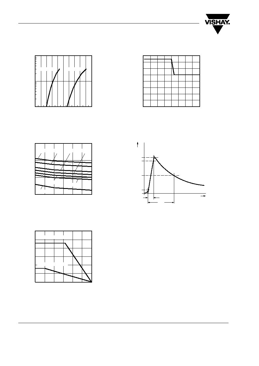
Figure 1. Forward Current vs. Forward Voltage
Figure 2. Typ. Diode Capacitance vs. Reverse Voltage
Figure 3. Power Dissipation vs. Ambient Temperature
0.10
1.00
10.00
0.6 0.7 0.8 0.9 1.0 1.1 1.2 1.3 1.4 1.5 1.6
17411
F
I ≠ Forward Current (
A
)
V
F
≠ Forward Voltage ( V )
Typ. V
F
Max. V
F
0.0
0.5
1.0
1.5
2.0
2.5
3.0
17412
C ≠
T
yp. Junction Capacitance ( pF )
D
10000
1000
10
100
V
R
≠ Reverse Voltage (V)
C5V1P
C6V8P
C12P
C27P
C51P
C200P
C18P
0.0
0.5
1.0
1.5
2.0
2.5
3.0
0
25
50
75
100
125
150
T
amb
≠ Ambient Temperature ( C )
17413
P
≠Power Dissipation ( W )
tot
ambient temperature
tie point temperature
Figure 4. Maximum Pulse Power Dissipation vs. Zener Voltage
Figure 5. Non-Repetitive Peak Reverse Current Pulse Definition
0
20
40
60
80
100
120
140
160
0
25
50
75
100 125 150 175 200
V
Znom
≠ Zener Voltage ( V )
17414
P
≠Max. Pulse Power Dissipation ( W )
RSM
17415
t
I
RSM
100
90
50
10
t
1
t
2
(%)
t
1
= 10
µs
t
2
= 1000
µ s