 | –≠–ª–µ–∫—Ç—Ä–æ–Ω–Ω—ã–π –∫–æ–º–ø–æ–Ω–µ–Ω—Ç: DG2003 | –°–∫–∞—á–∞—Ç—å:  PDF PDF  ZIP ZIP |
DG2003/2004/2005
Vishay Siliconix
New Product
Document Number: 71754
S-05298--Rev. B, 17-Dec-01
www.vishay.com
1
Low-Voltage Dual SPST Analog Switch
FEATURES
D
Low Voltage Operation (1.8 V to 5.5 V)
D
Low On-Resistance - r
DS(on
): 1.2
W
D
Fast Switching - 14 ns
D
Low Charge Injection - Q
INJ
: 1 pC
D
Low Power Consumption
D
TTL/CMOS Compatible
D
MSOP-8 Package
BENEFITS
D
Reduced Power Consumption
D
Simple Logic Interface
D
High Accuracy
D
Reduce Board Space
APPLICATIONS
D
Cellular Phones
D
Communication Systems
D
Portable Test Equipment
D
Battery Operated Systems
D
Sample and Hold Circuits
DESCRIPTION
The DG2003/2004/2005 are dual single-pole/single-throw
monolithic CMOS analog switch designed for high
performance switching of analog signals. Combining low
power, fast switching, low on-resistance (r
DS(on)
: 1.2
W
) and
small physical size (MSOP-8), the DG2003/2004/2005 are
ideal for portable and battery powered applications requiring
high performance and efficient use of board space.
The DG2003/2004/2005 are built on Vishay Siliconix's low
voltage JI2 process. An epitaxial layer prevents latchup.
Each switch conducts equally well in both directions when on,
and blocks up to the power supply level when off.
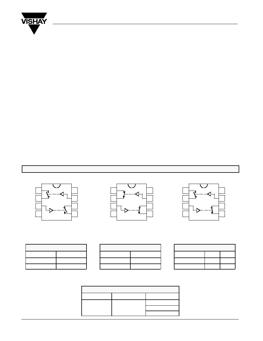
FUNCTIONAL BLOCK DIAGRAM AND PIN CONFIGURATION
NO
1
V+
COM
1
DG2005
IN
1
IN
2
COM
2
GND
NC
2
1
2
3
4
8
7
6
5
Top View
NC
1
V+
COM
1
DG2004
IN
1
IN
2
COM
2
GND
NC
2
1
2
3
4
8
7
6
5
Top View
NO
1
V+
COM
1
DG2003
IN
1
IN
2
COM
2
GND
NO
2
1
2
3
4
8
7
6
5
Top View
TRUTH TABLE - DG2003
TRUTH TABLE - DG2004
TRUTH TABLE - DG2005
Logic
NO
Logic
NC
Logic
NO
1
NC
2
0
Off
0
On
0
Off
On
1
On
1
Off
1
On
Off
ORDERING INFORMATION
Temp Range
Package
Part Number
DG2003DQ
-40 to 85
∞
C
MSOP-8
DG2004DQ
DG2005DQ
DG2003/2004/2005
Vishay Siliconix
New Product
www.vishay.com
2
Document Number: 71754
S-05298--Rev. B, 17-Dec-01
ABSOLUTE MAXIMUM RATINGS
Reference to GND
V+
-0.3 to +6 V
. . . . . . . . . . . . . . . . . . . . . . . . . . . . . . . . . . . . . . . . . . . . . . . . . . . .
IN, COM, NC, NO
a
-0.3 to (V+ + 0.3 V)
. . . . . . . . . . . . . . . . . . . . . . . . . . . . . . . . . . . . . . .
Continuous Current (Any terminal)
"
50 mA
. . . . . . . . . . . . . . . . . . . . . . . . . . .
Peak Current
"
200 mA
. . . . . . . . . . . . . . . . . . . . . . . . . . . . . . . . . . . . . . . . . . . . .
(Pulsed at 1 ms, 10% duty cycle)
Storage Temperature (D Suffix)
-65 to 150
∞
C
. . . . . . . . . . . . . . . . . . . . . . . . . . . .
Power Dissipation (Packages)
b
MSOP-8
c
320 mW
. . . . . . . . . . . . . . . . . . . . . . . . . . . . . . . . . . . . . . . . . . . . . . . . . .
Notes:
a.
Signals on NC, NO, or COM or IN exceeding V+ will be clamped by
internal diodes. Limit forward diode current to maximum current ratings.
b.
All leads welded or soldered to PC Board.
c.
Derate 6.5 mW/
_
C above 25
_
C
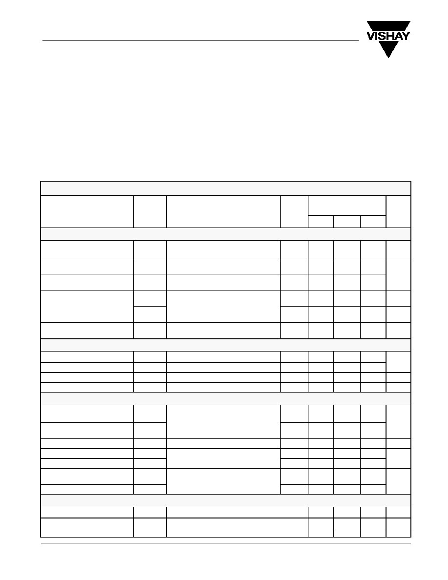
SPECIFICATIONS (V+ = 2.0 V)
Test Conditions
Otherwise Unless Specified
Limits
≠40 to 85
_
C
Parameter
Symbol
V+ = 2.0 V,
"
10%, V
IN
= 0.4 or 1.6 V
e
Temp
a
Min
b
Typ
c
Max
b
Unit
Analog Switch
Analog Signal Range
d
V
NO
, V
NC
,
V
COM
Full
0
V+
V
On-Resistance
r
ON
V+ = 2.0 V, V
COM
= 1.0 V, I
NO
, I
NC
= 1 mA
Room
Full
d
7.0
12.5
10.0
16.0
W
r
ON
Flatness
d
r
ON
Flatness
V+ = 2.0 V, V
COM
= 0 to V+, I
NO
, I
NC
= 1 mA
Room
5
W
I
NO(off),
I
NC(off)
V+ = 2.2 V
Room
Full
d
≠500
≠4.0
500
4.0
pA
nA
Switch Off Leakage Current
f
I
COM(off)
V+ = 2.2 V
V
NO,
V
NC
= 0.5 V/1.5 V, V
COM
= 1.5 V/0.5 V
Room
Full
d
≠500
≠4.0
500
4.0
pA
nA
Channel-On Leakage Current
f
I
COM(on)
V+ = 2.2 V, V
NO,
V
NC
= V
COM
= 0.5 V/1.5 V
Room
Full
d
≠500
≠4.0
500
4.0
pA
nA
Digital Control
Input High Voltage
V
INH
Full
1.6
Input Low Voltage
V
INL
Full
0.4
V
Input Capacitance
d
C
in
Full
5
pF
Input Current
I
INL
or I
INH
V
IN
= 0 or V+
Full
≠1
1
m
A
Dynamic Characteristics
Turn-On Time
t
ON
V
NO
or V
NC
= 1.5 V, R
L
= 300
W
, C
L
= 35 pF
Room
Full
d
30
47
48
Turn-Off Time
t
OFF
V
NO
or V
NC
= 1.5 V, R
L
= 300
W
, C
L
= 35 pF
Figures 1 and 2
Room
Full
d
22
37
48
ns
Charge Injection
d
Q
INJ
C
L
= 1 nF, V
GEN
= 0 V, R
GEN
= 0
W
, Figure 3
Room
2
pC
Off-Isolation
d
OIRR
W
Room
≠61
Crosstalk
d
X
TALK
R
L
= 50
W
, C
L
= 5 pF, f = 1 MHz
Room
≠67
dB
NO, NC Off Capacitance
d
C
NO(off),
C
NC(off)
V
IN
= 0 or V+, f = 1 MHz
Room
53
pF
Channel-On Capacitance
d
C
ON
V
IN
= 0 or V+, f = 1 MHz
Room
110
pF
Power Supply
Power Supply Range
V+
1.8
2.2
V
Power Supply Current
d
I+
0.02
1.0
m
A
Power Consumption
P
C
V
IN
= 0 or V+
2.2
m
W
DG2003/2004/2005
Vishay Siliconix
New Product
Document Number: 71754
S-05298--Rev. B, 17-Dec-01
www.vishay.com
3
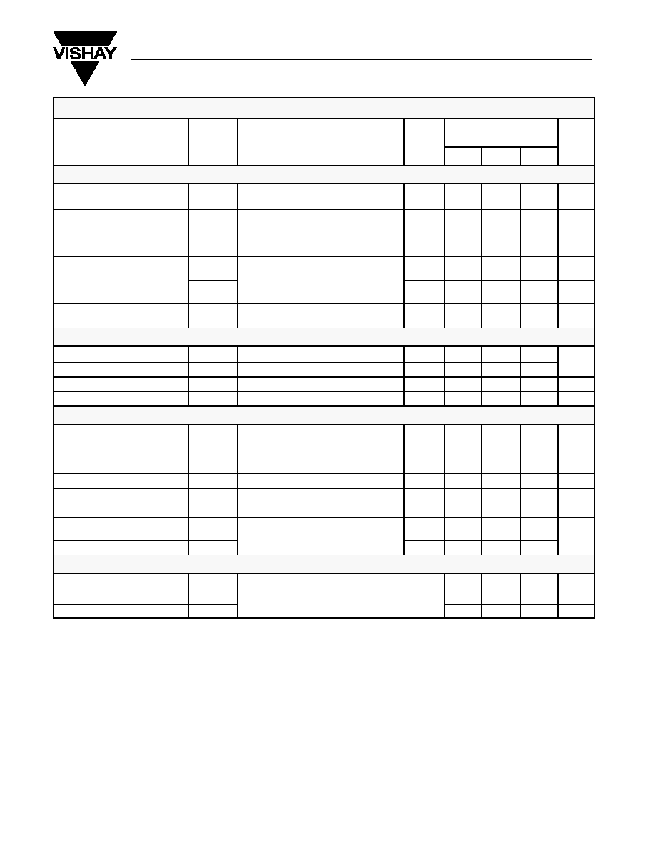
SPECIFICATIONS (V+ = 3.0 V)
Test Conditions
Otherwise Unless Specified
Limits
≠40 to 85
_
C
Parameter
Symbol
V+ = 3 V,
"
10%, V
IN
= 0.4 or 2.0 V
e
Temp
a
Min
b
Typ
c
Max
b
Unit
Analog Switch
Analog Signal Range
d
V
NO
, V
NC
,
V
COM
Full
0
V+
V
On-Resistance
r
ON
V+ = 2.7 V, V
COM
= 1.5 V, I
NO
, I
NC
= 10 mA
Room
Full
2.2
2.4
3.5
3.7
W
r
ON
Flatness
d
r
ON
Flatness
V+ = 2.7 V, V
COM
= 0 to V+, I
NO
, I
NC
= 10 mA
Room
0.5
W
I
NO(off),
I
NC(off)
V+ = 3.3 V
Room
Full
≠500
≠6.0
500
6.0
pA
nA
Switch Off Leakage Current
f
I
COM(off)
V+ = 3.3 V
V
NO,
V
NC
= 1 V/3 V, V
COM
= 3 V/1 V
Room
Full
≠500
≠6.0
500
6.0
pA
nA
Channel-On Leakage Current
f
I
COM(on)
V+ = 3.3 V, V
NO,
V
NC
= V
COM
= 1 V/3 V
Room
Full
≠500
≠6.0
500
6.0
pA
nA
Digital Control
Input High Voltage
V
INH
Full
2
Input Low Voltage
V
INL
Full
0.4
V
Input Capacitance
d
C
in
Full
5
pF
Input Current
I
INL
or I
INH
V
IN
= 0 or V+
Full
≠1
1
m
A
Dynamic Characteristics
Turn-On Time
d
t
ON
V
NO
or V
NC
= 2.0 V, R
L
= 300
W
, C
L
= 35 pF
Room
Full
19
35
36
Turn-Off Time
d
t
OFF
V
NO
or V
NC
= 2.0 V, R
L
= 300
W
, C
L
= 35 pF
Figure 1 and 2
Room
Full
17
31
34
ns
Charge Injection
d
Q
INJ
C
L
= 1 nF, V
GEN
= 0 V, R
GEN
= 0
W
, Figure 3
Room
1
pC
Off-Isolation
d
OIRR
W
Room
≠61
Crosstalk
d
X
TALK
R
L
= 50
W
, C
L
= 5 pF, f = 1 MHz
Room
≠67
dB
NO, NC Off Capacitance
d
C
NO(off),
C
NC(off)
V
IN
= 0 or V+, f = 1 MHz
Room
53
pF
Channel-On Capacitance
d
C
ON
V
IN
= 0 or V+, f = 1 MHz
Room
110
pF
Power Supply
Power Supply Range
V+
2.7
3.3
V
Power Supply Current
I+
0.02
1.0
m
A
Power Consumption
P
C
V
IN
= 0 or V+
3.3
m
W
DG2003/2004/2005
Vishay Siliconix
New Product
www.vishay.com
4
Document Number: 71754
S-05298--Rev. B, 17-Dec-01
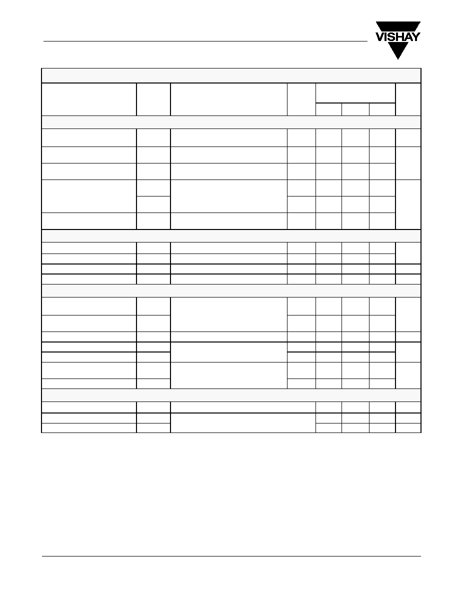
SPECIFICATIONS (V+ = 5.0 V)
Test Conditions
Otherwise Unless Specified
Limits
≠40 to 85
_
C
Parameter
Symbol
V+ = 5 V,
"
10%, V
IN
= 0.8 or 2.4 V
e
Temp
a
Min
b
Typ
c
Max
b
Unit
Analog Switch
Analog Signal Range
d
V
NO
, V
NC
,
V
COM
Full
0
V+
V
On-Resistance
r
ON
V+ = 4.5 V, V
COM
= 3 V, I
NO
, I
NC
= 10 mA
Room
Full
1.2
1.6
2.5
2.7
W
r
ON
Flatness
d
r
ON
Flatness
V+ = 4.5 V, V
COM
= 0 to V+, I
NO
, I
NC
= 10 mA
Room
0.2
W
I
NO(off),
I
NC(off)
V+ = 5.5 V
Room
Full
≠1.0
≠8.0
1.0
8.0
Switch Off Leakage Current
I
COM(off)
V+ = 5.5 V
V
NO,
V
NC
= 1 V/4.5 V, V
COM
= 4.5 V/1 V
Room
Full
≠1.0
≠8.0
1.0
8.0
nA
Channel-On Leakage Current
I
COM(on)
V+ = 5.5 V, V+ = 5.5 V
V
NO,
V
NC
= V
COM
= 1 V/4.5 V
Room
Full
≠1.0
≠8.0
1.0
8.0
Digital Control
Input High Voltage
V
INH
Full
2.4
Input Low Voltage
V
INL
Full
0.8
V
Input Capacitance
C
in
Full
5
pF
Input Current
I
INL
or I
INH
V
IN
= 0 or V+
Full
≠1
1
m
A
Dynamic Characteristics
Turn-On Time
d
t
ON
V
NO
or V
NC
= 3 V, R
L
= 300
W
, C
L
= 35 pF
Room
Full
13
28
31
Turn-Off Time
d
t
OFF
V
NO
or V
NC
= 3 V, R
L
= 300
W
, C
L
= 35 pF
Figure 1 and 2
Room
Full
19
22
31
ns
Charge Injection
d
Q
INJ
C
L
= 1 nF, V
GEN
= 0 V, R
GEN
= 0
W
, Figure 3
Room
1
pC
Off-Isolation
d
OIRR
W
Room
≠61
Crosstalk
d
X
TALK
R
L
= 50
W
, C
L
= 5 pF, f = 1 MHz
Room
≠67
dB
Source-Off Capacitance
d
C
NO(off),
C
NC(off)
V
IN
= 0 or V+, f = 1 MHz
Room
51
pF
Channel-On Capacitance
d
C
ON
V
IN
= 0 or V+, f = 1 MHz
Room
110
pF
Power Supply
Power Supply Range
V+
4.5
5.5
V
Power Supply Current
I+
0.02
1.0
m
A
Power Consumption
P
C
V
IN
= 0 or V+
5.5
m
W
Notes:
a.
Room = 25
∞
C, Full = as determined by the operating suffix.
b.
The algebraic convention whereby the most negative value is a minimum and the most positive a maximum, is used in this data sheet.
c.
Typical values are for design aid only, not guaranteed nor subject to production testing.
d.
Guarantee by design, nor subjected to production test.
e.
V
IN
= input voltage to perform proper function.
f.
Guaranteed by 5-V leakage testing, not production tested.
DG2003/2004/2005
Vishay Siliconix
New Product
Document Number: 71754
S-05298--Rev. B, 17-Dec-01
www.vishay.com
5
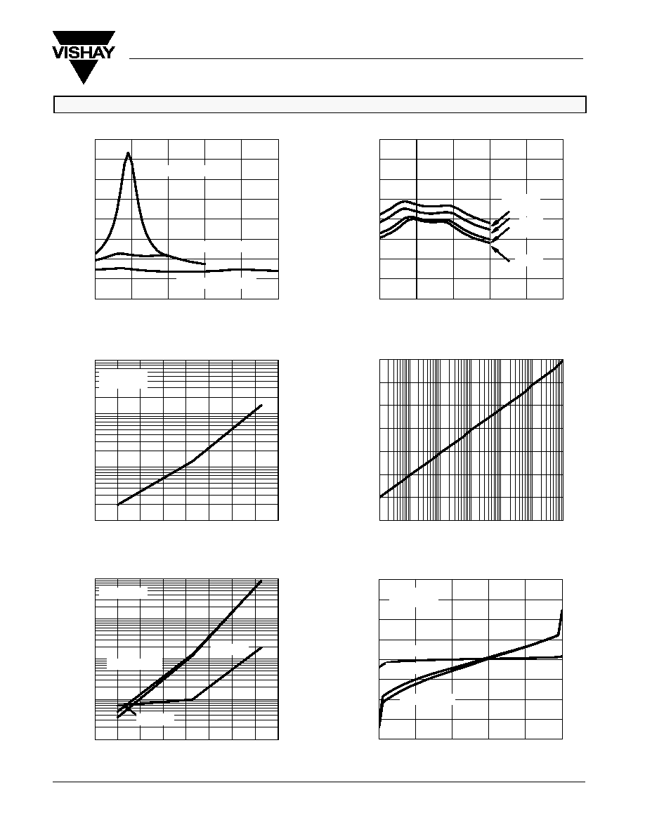
TYPICAL CHARACTERISTICS (25_C UNLESS NOTED)
10 m
≠60
≠40
≠20
0
20
40
60
80
100
1000
1
100
≠60
≠40
≠20
0
20
40
60
80
100
Supply Current vs. Input Switching Frequency
Input Switching Frequency (Hz)
10 K
1 M
10 M
100 K
1 K
100
10
10
1
0.01
Supply Current vs. Temperature
Temperature (
_
C)
I+
≠
Supply Current (nA)
≠
On-Resistance (
r
ON
W
)
0.0
0.5
1.0
1.5
2.0
2.5
3.0
3.5
4.0
0
1
2
3
4
5
0
1
2
3
4
5
6
7
8
0
1
2
3
4
5
≠200
≠150
≠100
≠50
0
50
100
150
200
0
1
2
3
4
5
Leakage Current vs. Temperature
Leakage vs. Analog Voltage
V
COM
, V
NO
, V
NC
≠ Analog Voltage
r
ON
vs. V
COM
Supply Voltage
V
COM
≠ Analog Voltage (V)
V+ = 2 V/I
S
= 1 mA
V+ = 3 V/I
S
= 100 mA
V+ = 5 V/I
S
= 100 mA
r
ON
vs. Analog Voltage and Temperature
≠
On-Resistance (
r
ON
W
)
V
COM
≠ Analog Voltage (V)
V+ = 3 V
≠40
_
C
25
_
C
0
_
C
0.1
V+ = 5 V
V
IN
= 0 V
I+
≠
Supply Current (A)
Leakage Current (pA)
Temperature (
_
C)
10000
V+ = 5 V
10
I
NO(off)
/I
NC(off)
I
COM(on)
I
COM(off)
Leakage Current (pA)
V+ = 5 V
T = 25
_
C
I
NO(off)
/I
NC(off)
I
COM(on)
I
COM(off)
1 n
1 m
100
m
10
m
1
m
10 n
100 n
85
_
C