DG2041/2042/2043
Vishay Siliconix
New Product
Document Number: 72091
S-03008--Rev. A, 20-Jan-03
www.vishay.com
1
Low-Voltage, Low r
ON
Quad SPST Analog Switch
FEATURES
D
Low Voltage Operation (1.8 V to 5.5 V)
D
Low On-Resistance - r
DS(on
): 1.0
W
D
Fast Switching - 14 ns t
ON
D
Low Charge Injection - Q
INJ
: 1 pC
D
Low Power Consumption
D
TTL/CMOS Compatible
D
TSSOP-16 and QFN-16 Packages
BENEFITS
D
Reduced Power Consumption
D
Simple Logic Interface
D
High Accuracy
D
Reduce Board Space
APPLICATIONS
D
Cellular Phones
D
Communication Systems
D
Portable Test Equipment
D
Battery Operated Systems
D
Sample and Hold Circuits
DESCRIPTION
The DG2041/2042/2043 are quad single-pole/single-throw
monolithic CMOS analog switch designed for high
performance switching of analog signals. Combining low
power, fast switching, low on-resistance (r
DS(on)
:
1.0
W
@
2.7
V) and small physical size, the
DG2041/2042/2043 are ideal for portable and battery powered
applications requiring high performance and efficient use of
board space.
The DG2041/2042/2043 are built on Vishay Siliconix's new
high density low voltage process. An epitaxial layer prevents
latchup.
Each switch conducts equally well in both directions when on,
and blocks up to the power supply level when off.
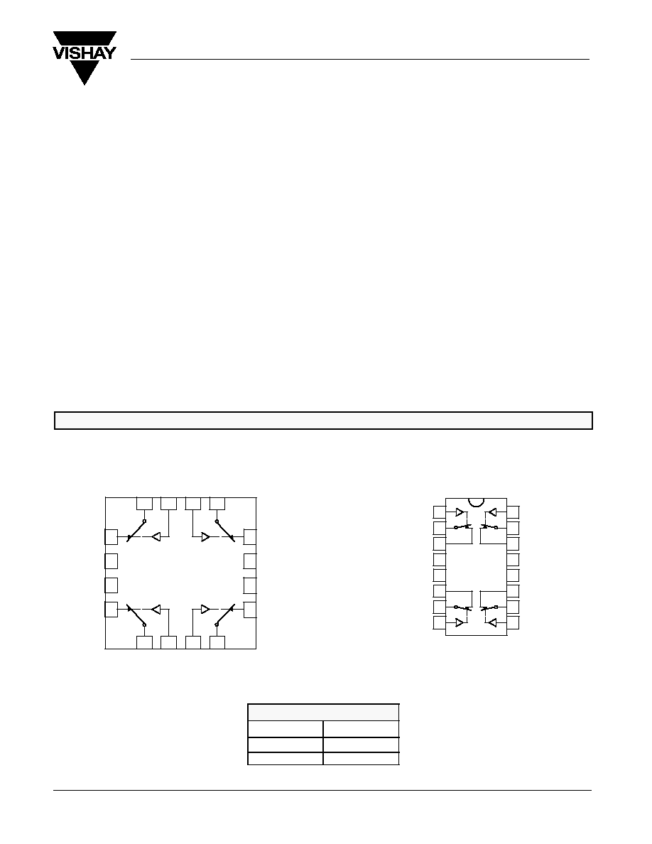
FUNCTIONAL BLOCK DIAGRAM AND PIN CONFIGURATION DG2041
DG2041DN
N.C.
V+
NC4
GND
NC3
N.C.
NC1
NC2
1
2
3
12
11
10
4
9
5
6
7
8
16
15
14
13
Top View
QFN-16 (4 X 4)
COM1
IN1
IN2
COM2
COM4
IN4
IN3
COM3
1
2
3
4
5
6
7
8
16
15
14
13
12
11
10
9
Top View
IN1
IN2
COM1
COM2
NC1
NC2
N.C.
V+
GND
N.C.
NC4
NC3
COM4
COM3
IN4
IN3
TSSOP
DG2041DQ
TRUTH TABLE DG2041
Logic
Switch
0
On
1
Off
Switches Shown for Logic "0" Input
DG2041/2042/2043
Vishay Siliconix
New Product
www.vishay.com
2
Document Number: 72091
S-03008--Rev. A, 20-Jan-03
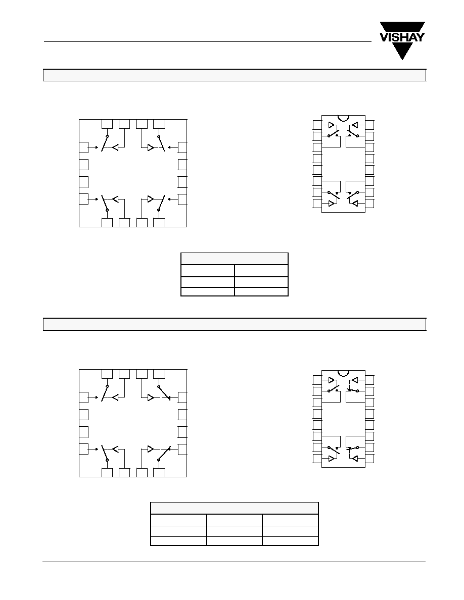
FUNCTIONAL BLOCK DIAGRAM AND PIN CONFIGURATION DG2042
DG2042DN
N.C.
V+
NO4
GND
NO3
N.C.
NO1
NO2
1
2
3
12
11
10
4
9
5
6
7
8
16
15
14
13
Top View
QFN-16 (4 X 4)
COM1
IN1
IN2
COM2
COM4
IN4
IN3
COM3
1
2
3
4
5
6
7
8
16
15
14
13
12
11
10
9
Top View
IN1
IN2
COM1
COM2
NO1
NO2
N.C.
V+
GND
N.C.
NO4
NO3
COM4
COM3
IN4
IN3
TSSOP
DG2042DQ
TRUTH TABLE DG2042
Logic
Switch
0
Off
1
On
Switches Shown for Logic "0" Input
FUNCTIONAL BLOCK DIAGRAM AND PIN CONFIGURATION DG2043
DG2043DN
N.C.
V+
NO4
GND
NC3
N.C.
NO1
NC2
1
2
3
12
11
10
4
9
5
6
7
8
16
15
14
13
Top View
QFN-16 (4 X 4)
COM1
IN1
IN2
COM2
COM4
IN4
IN3
COM3
1
2
3
4
5
6
7
8
16
15
14
13
12
11
10
9
Top View
IN1
IN2
COM1
COM2
NO1
NC2
N.C.
V+
GND
N.C.
NO4
NC3
COM4
COM3
IN4
IN3
TSSOP
DG2043DQ
TRUTH TABLE DG2043
Logic
Switches 1, 4
Switches 2, 3
0
Off
On
1
On
Off
Switches Shown for Logic "0" Input
DG2041/2042/2043
Vishay Siliconix
New Product
Document Number: 72091
S-03008--Rev. A, 20-Jan-03
www.vishay.com
3
ORDERING INFORMATION
Temp Range
Package
Part Number
DG2041DQ
TSSOP-16
DG2042DQ
�
DG2043DQ
-40 to 85
�
C
DG2041DN
QFN-16
(4x4 mm)
DG2042DN
(4x4 mm)
DG2043DN
ABSOLUTE MAXIMUM RATINGS
Reference to GND
V+
-0.3 to +6 V
. . . . . . . . . . . . . . . . . . . . . . . . . . . . . . . . . . . . . . . . . . . . . . . . . . . .
IN, COM, NC, NO
a
-0.3 to (V+ + 0.3 V)
. . . . . . . . . . . . . . . . . . . . . . . . . . . . . . . . . . . . . . .
Continuous Current (Any terminal)
"
50 mA
. . . . . . . . . . . . . . . . . . . . . . . . . . .
Peak Current
"
200 mA
. . . . . . . . . . . . . . . . . . . . . . . . . . . . . . . . . . . . . . . . . . . . .
(Pulsed at 1 ms, 10% duty cycle)
Storage Temperature (D Suffix)
-65 to 150
�
C
. . . . . . . . . . . . . . . . . . . . . . . . . . . .
Power Dissipation (Packages)
b
TSSOP-16
c
450 mW
. . . . . . . . . . . . . . . . . . . . . . . . . . . . . . . . . . . . . . . . . . . . . . . .
QFN-16 (4 x 4 mm)
d
1880 mW
. . . . . . . . . . . . . . . . . . . . . . . . . . . . . . . . . . . . . . .
Notes:
a.
Signals on NC, NO, or COM or IN exceeding V+ will be clamped by
internal diodes. Limit forward diode current to maximum current ratings.
b.
All leads welded or soldered to PC Board.
c.
Derate 5.6 mW/
_
C above 70
_
C
d.
Derate 23.5 mW/
_
C above 70
_
C
e.
Manual soldering with soldering iron is not recommended for leadless
components. The QFN is a leadless package. The end of the lead termi-
nal is exposed copper (not plated) as a result of the singulation process
in manufacturing. A solder fillet at the exposed copper lip cannot be
guaranteed and is not required to ensure adequate bottom side solder
interconnection.
SPECIFICATIONS (V+ = 2.0 V)
Test Conditions
Otherwise Unless Specified
Limits
- 40 to 85
_
C
Parameter
Symbol
V+ = 2.0 V, V
IN
= 0.4 or 1.6 V
e
Temp
a
Min
b
Typ
c
Max
b
Unit
Analog Switch
Analog Signal Range
d
V
NO
, V
NC
,
V
COM
Full
0
V+
V
On-Resistance
r
ON
V+ = 2.0 V, V
COM
= 0.2 V/1.2 V, I
NO
, I
NC
=
10 mA
Room
Full
d
3.0
6.3
6.3
r
ON
Flatness
d
r
ON
Flatness
V+ = 2.0 V, V
COM
= 0 to V+, I
NO
, I
NC
= 10 mA
Room
4.2
W
r
ON Match Between Channels
D
r
ON
V+ = 2.0 V, V
COM
= 0 to V+, I
NO
, I
NC
= 10 mA
Room
0.4
I
NO(off),
I
NC(off)
V+ = 2.2 V
Room
Full
d
- 1
- 10
1
10
Switch Off Leakage Current
f
I
COM(off)
V+ = 2.2 V
V
NO,
V
NC
= 0.2 V/2.0 V, V
COM
= 2.0 V/0.2 V
Room
Full
d
- 1
- 10
1
10
nA
Channel-On Leakage Current
f
I
COM(on)
V+ = 2.2 V, V
NO,
V
NC
= V
COM
= 0.2 V/2.0 V
Room
Full
d
- 1
- 10
1
10
Digital Control
Input High Voltage
V
INH
Full
1.6
Input Low Voltage
V
INL
Full
0.4
V
Input Capacitance
d
C
in
Full
4
pF
Input Current
I
INL
or I
INH
V
IN
= 0 or V+
Full
- 1
1
m
A
DG2041/2042/2043
Vishay Siliconix
New Product
www.vishay.com
4
Document Number: 72091
S-03008--Rev. A, 20-Jan-03
SPECIFICATIONS (V+ = 2.0 V)
Parameter
Limits
- 40 to 85
_
C
Temp
a
Test Conditions
Otherwise Unless Specified
Symbol
Parameter
Unit
Max
b
Typ
c
Min
b
Temp
a
V+ = 2.0 V, V
IN
= 0.4 or 1.6 V
e
Symbol
Dynamic Characteristics
Turn-On Time
t
ON
V
NO
or V
NC
= 1.5 V, R
L
= 300
W
, C
L
= 35 pF
Room
Full
d
30
81
82
Turn-Off Time
t
OFF
V
NO
or V
NC
= 1.5 V, R
L
= 300
W
, C
L
= 35 pF
Figures 1 and 2
Room
Full
d
22
41
42
ns
Break-Before-Make Time Delay
t
D
V
NO
or V
NC
= 1.5 V, R
L
- 300
W
, C
L
- 35 pF
(DG2043 Only)
Room
5
Charge Injection
d
Q
INJ
C
L
= 1 nF, V
GEN
= 0 V, R
GEN
= 0
W
, Figure 2
Room
1
pC
Off-Isolation
d
OIRR
W
Room
- 63
Crosstalk
d
X
TALK
R
L
= 50
W
, C
L
= 5 pF, f = 1 MHz
Room
- 95
dB
NO, NC Off Capacitance
d
C
NO(off),
C
NC(off)
V
IN
= 0 or V+, f = 1 MHz
Room
24
pF
Channel-On Capacitance
d
C
ON
V
IN
= 0 or V+, f = 1 MHz
Room
48
pF
Power Supply
Power Supply Current
d
I+
V
IN
= 0 or V+
0.001
1.0
m
A
SPECIFICATIONS (V+ = 3.0 V)
Test Conditions
Otherwise Unless Specified
Limits
- 40 to 85
_
C
Parameter
Symbol
V+ = 3 V,
"
10%, V
IN
= 0.4 or 2.0 V
e
Temp
a
Min
b
Typ
c
Max
b
Unit
Analog Switch
Analog Signal Range
d
V
NO
, V
NC
,
V
COM
Full
0
V+
V
On-Resistance
r
ON
V+ = 2.7 V, V
COM
= 0.7 V/1.5 V, I
NO
,
I
NC
= 10 mA
Room
Full
1.6
2.1
2.2
r
ON
Flatness
d
r
ON
Flatness
V+ = 2.7 V, V
COM
= 0 to V+, I
NO
, I
NC
= 10 mA
Room
0.7
W
r
ON
Match Between Channels
D
r
ON
V+ = 2.7 V, V
COM
= 0 to V+, I
NO
, I
NC
= 10 mA
Room
0.3
I
NO(off),
I
NC(off)
V+ = 3.3 V
Room
Full
- 1
- 10
1
10
Switch Off Leakage Current
f
I
COM(off)
V+ = 3.3 V
V
NO,
V
NC
= 0.3 V/3.0 V, V
COM
= 3.0 V/0.3 V
Room
Full
- 1
- 10
1
10
nA
Channel-On Leakage Current
f
I
COM(on)
V+ = 3.3 V, V
NO,
V
NC
= V
COM
= 0.3 V/3.0 V
Room
Full
- 1
- 10
1
10
Digital Control
Input High Voltage
d
V
INH
Full
1.6
Input Low Voltage
V
INL
Full
0.4
V
Input Capacitance
d
C
in
Full
4
pF
Input Current
I
INL
or I
INH
V
IN
= 0 or V+
Full
- 1
1
m
A

DG2041/2042/2043
Vishay Siliconix
New Product
Document Number: 72091
S-03008--Rev. A, 20-Jan-03
www.vishay.com
5
SPECIFICATIONS (V+ = 3.0 V)
Parameter
Limits
- 40 to 85
_
C
Temp
a
Test Conditions
Otherwise Unless Specified
Symbol
Parameter
Unit
Max
b
Typ
c
Min
b
Temp
a
V+ = 3 V,
"
10%, V
IN
= 0.4 or 2.0 V
e
Symbol
Dynamic Characteristics
Turn-On Time
d
t
ON
V
NO
or V
NC
= 2.0 V, R
L
= 300
W
, C
L
= 35 pF
Room
Full
19
51
52
Turn-Off Time
d
t
OFF
V
NO
or V
NC
= 2.0 V, R
L
= 300
W
, C
L
= 35 pF
Figure 1 and 2
Room
Full
17
36
37
ns
Break-Before-Make Time Delay
t
D
V
NO
or V
NC
= 2.0 V, R
L
- 300
W
, C
L
- 35 pF
(DG2043 Only)
Room
2
Charge Injection
d
Q
INJ
C
L
= 1 nF, V
GEN
= 0 V, R
GEN
= 0
W
, Figure 2
Room
3
pC
Off-Isolation
d
OIRR
W
Room
- 63
Crosstalk
d
X
TALK
R
L
= 50
W
, C
L
= 5 pF, f = 1 MHz
Room
- 94
dB
NO, NC Off Capacitance
d
C
NO(off),
C
NC(off)
V
IN
= 0 or V+, f = 1 MHz
Room
25
pF
Channel-On Capacitance
d
C
ON
V
IN
= 0 or V+, f = 1 MHz
Room
49
pF
Power Supply
Power Supply Current
I+
V
IN
= 0 or V+
0.001
1.0
m
A
SPECIFICATIONS (V+ = 5.0 V)
Test Conditions
Otherwise Unless Specified
Limits
- 40 to 85
_
C
Parameter
Symbol
V+ = 5 V,
"
10%, V
IN
= 0.8 or 2.4 V
e
Temp
a
Min
b
Typ
c
Max
b
Unit
Analog Switch
Analog Signal Range
d
V
NO
, V
NC
,
V
COM
Full
0
V+
V
On-Resistance
r
ON
V+ = 4.5 V, V
COM
= 0.7 V/2.5 V, I
NO
,
I
NC
= 10 mA
Room
Full
1.0
1.5
1.6
r
ON
Flatness
d
r
ON
Flatness
V+ = 4.5 V, V
COM
= 0 to V+, I
NO
, I
NC
= 10 mA
Room
0.7
W
r
ON
Match Between Channels
D
r
ON
V+ = 4.5 V, V
COM
= 0 to V+, I
NO
, I
NC
= 10 mA
Room
0.3
I
NO(off),
I
NC(off)
V+ = 5.5 V
Room
Full
- 1.0
- 10
1.0
10
Switch Off Leakage Current
I
COM(off)
V+ = 5.5 V
V
NO,
V
NC
= 1 V/4.5 V, V
COM
= 4.5 V/1 V
Room
Full
- 1.0
- 10
1.0
10
nA
Channel-On Leakage Current
I
COM(on)
V+ = 5.5 V, V
NO,
V
NC
= V
COM
= 1 V/4.5 V
Room
Full
- 1.0
- 10
1.0
10
Digital Control
Input High Voltage
V
INH
Full
2.4
Input Low Voltage
V
INL
Full
0.8
V
Input Capacitance
C
in
Full
4
pF
Input Current
I
INL
or I
INH
V
IN
= 0 or V+
Full
- 1
1
m
A