 | –≠–ª–µ–∫—Ç—Ä–æ–Ω–Ω—ã–π –∫–æ–º–ø–æ–Ω–µ–Ω—Ç: DG211BDJ | –°–∫–∞—á–∞—Ç—å:  PDF PDF  ZIP ZIP |
IN
1
IN
2
D
1
D
2
S
1
S
2
V≠
V+
GND
V
L
S
4
S
3
D
4
D
3
IN
4
IN
3
1
2
3
4
5
6
7
8
16
15
14
13
12
11
10
9
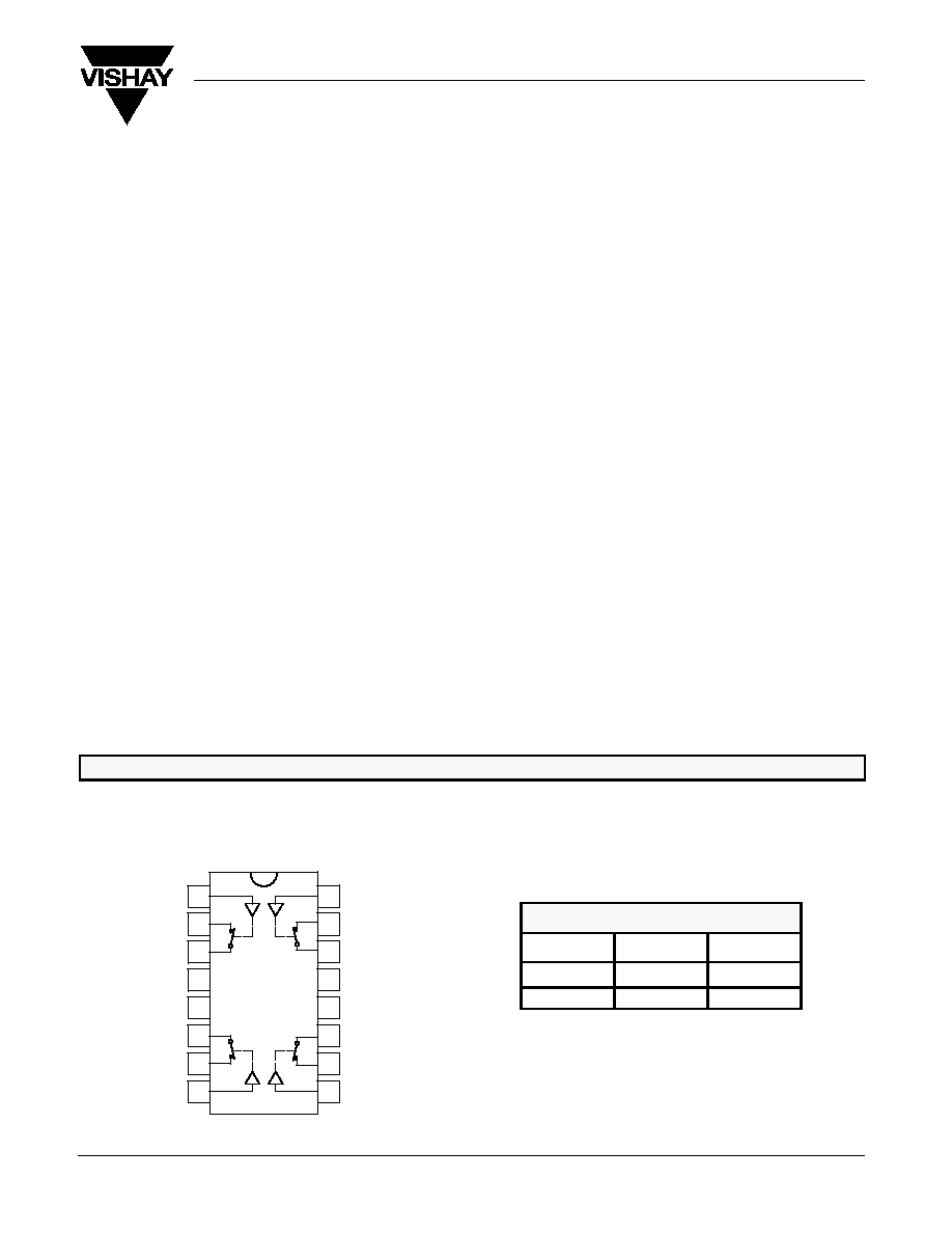
Top View
DG211B
Dual-In-Line, SOIC and TSSOP
DG211B/212B
Vishay Siliconix
Document Number: 70040
S-00788--Rev. H, 24-Apr-00
www.vishay.com
S
FaxBack 408-970-5600
4-1
Improved Quad CMOS Analog Switches
FEATURES
BENEFITS
APPLICATIONS
D "
22-V Supply Voltage Rating
D
TTL and CMOS Compatible Logic
D
Low On-Resistance--r
DS(on)
: 50
W
D
Low Leakage--I
D(on)
: 20 pA
D
Single Supply Operation Possible
D
Extended Temperature Range
D
Fast Switching--t
ON
: 120 ns
D
Low Charge Injection--Q: 1 pC
D
Wide Analog Signal Range
D
Simple Logic Interface
D
Higher Accuracy
D
Minimum Transients
D
Reduced Power Consumption
D
Superior to DG211/212
D
Space Savings (TSSOP)
D
Industrial Instrumentation
D
Test Equipment
D
Communications Systems
D
Disk Drives
D
Computer Peripherals
D
Portable Instruments
D
Sample-and-Hold Circuits
DESCRIPTION
The DG211B/212B analog switches are highly improved
versions of the industry-standard DG211/212. These devices
are fabricated in Vishay Siliconix' proprietary silicon gate
CMOS process, resulting in lower on-resistance, lower
leakage, higher speed, and lower power consumption.
These quad single-pole single-throw switches are designed
for a wide variety of applications in telecommunications,
instrumentation, process control, computer peripherals, etc. An
improved charge injection compensation design minimizes
switching transients. The DG211B and DG212B can handle
up to
"
22 V, and have an improved continuous current rating
of 30 mA. An epitaxial layer prevents latchup.
All devices feature true bi-directional performance in the on
condition, and will block signals to the supply levels in the off
condition.
The DG211B is a normally closed switch and the DG212B is
a normally open switch. (See Truth Table.)
FUNCTIONAL BLOCK DIAGRAM AND PIN CONFIGURATION
TRUTH TABLE
Logic
DG211B
DG212B
0
ON
OFF
1
OFF
ON
Logic "0"
v
0.8 V
Logic "1"
w
2.4 V
DG211B/212B
Vishay Siliconix
www.vishay.com
S
FaxBack 408-970-5600
4-2
Document Number: 70040
S-00788--Rev. H, 24-Apr-00
ORDERING INFORMATION
Temp Range
Package
Part Number
40
85 C
16-Pin Plastic DIP
DG211BDJ
40
85 C
16-Pin Plastic DIP
DG212BDJ
≠40 to 85
_
C
16-Pin Narrow SOIC
DG211BDY
≠40 to 85
_
C
16-Pin Narrow SOIC
DG212BDY
16-Pin TSSOP
DG211BDQ
16-Pin TSSOP
DG212BDQ
ABSOLUTE MAXIMUM RATINGS
Voltages Referenced to V≠
V+
44 V
. . . . . . . . . . . . . . . . . . . . . . . . . . . . . . . . . . . . . . . . . . . . . . . . . . . . . . . . . . .
GND
25 V
. . . . . . . . . . . . . . . . . . . . . . . . . . . . . . . . . . . . . . . . . . . . . . . . . . . . . . . . .
Digital Inputs
a
V
S
, V
D
(V≠) ≠2 V to (V+) +2 V
. . . . . . . . . . . . . . . . . . . . . . . . . .
or 30 mA, whichever occurs first
Current, Any Terminal
30 mA
. . . . . . . . . . . . . . . . . . . . . . . . . . . . . . . . . . . . . . . .
Peak Current, S or D
(Pulsed at 1 ms, 10% duty cycle max)
100 mA
. . . . . . . . . . . . . . . . . . . . . . . . .
Storage Temperature
≠65 to 125
_
C
. . . . . . . . . . . . . . . . . . . . . . . . . . . . . . . . . .
Power Dissipation (Package)b
16-Pin Plastic DIP
c
470 mW
. . . . . . . . . . . . . . . . . . . . . . . . . . . . . . . . . . . . . . . . .
16-Pin Narrow SOIC and TSSOP
d
640 mW
. . . . . . . . . . . . . . . . . . . . . . . . . . . .
Notes:
a.
Signals on S
X
, D
X
, or IN
X
exceeding V+ or V≠ will be clamped by internal
diodes. Limit forward diode current to maximum current ratings.
b.
All leads welded or soldered to PC Board.
c.
Derate 6.5 mW/
_
C above 75
_
C
d.
Derate 7.6 mW/
_
C above 75
_
C
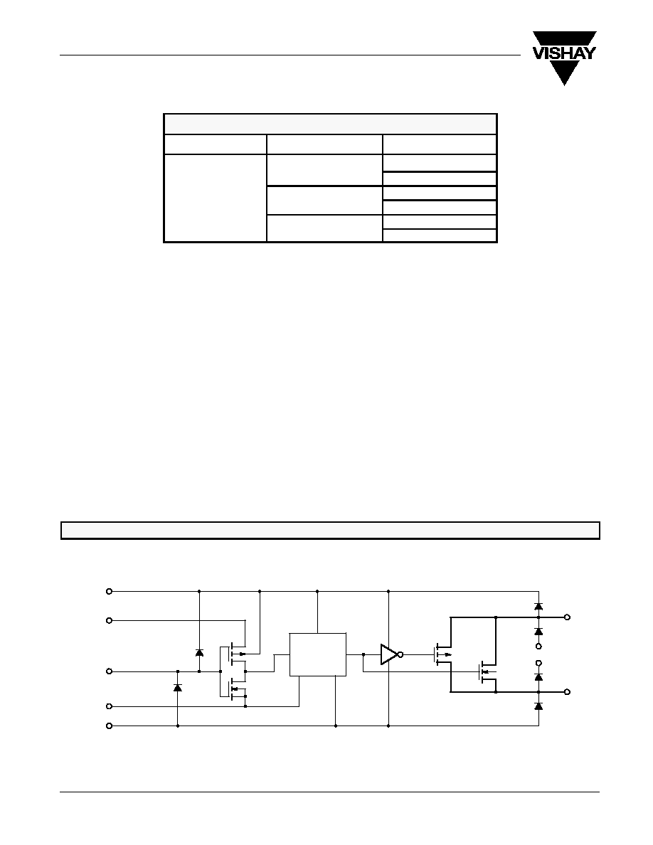
SCHEMATIC DIAGRAM (TYPICAL CHANNEL)
FIGURE 1.
D
X
S
X
V+
IN
X
V≠
Level
Shift/
GND
V+
V≠
Drive
V
L

DG211B/212B
Vishay Siliconix
Document Number: 70040
S-00788--Rev. H, 24-Apr-00
www.vishay.com
S
FaxBack 408-970-5600
4-3
SPECIFICATIONS
Test Conditions
Unless Otherwise Specified
D Suffix
≠40 to 85
_
C
Parameter
Symbol
V+ = 15 V, V≠ = ≠15 V
V
L
= 5 V, V
IN
= 2.4 V, 0.8 V
e
Temp
a
Min
b
Typ
c
Max
b
Unit
Analog Switch
Analog Signal Range
d
V
ANALOG
Full
≠15
15
V
Drain-Source On-Resistance
r
DS(on)
V
D
=
"
10 V, I
S
= 1 mA
Room
Full
45
85
100
W
r
DS(on)
Match
D
r
DS(on)
D
,
S
Room
2
Source Off Leakage Current
I
S(off)
V
S
=
"
14 V, V
D
=
#
14 V
Room
Full
≠0.5
≠5
"
0.01
0.5
5
A
Drain Off Leakage Current
I
D(off)
V
D
=
"
14 V, V
S
=
#
14 V
Room
Full
≠0.5
≠5
"
0.01
0.5
5
nA
Drain On Leakage Current
I
D(on)
V
S
= V
D
=
"
14 V
Room
Full
≠0.5
≠10
"
0.02
0.5
10
Digital Control
Input Voltage High
V
INH
Full
2.4
V
Input Voltage Low
V
INL
Full
0.8
V
Input Current
I
INH
or I
INL
V
INH
or V
INL
Full
≠1
1
m
A
Input Capacitance
C
IN
Room
5
pF
Dynamic Characteristics
Turn-On Time
t
ON
V
S
=10 V
S
Fi
2
Room
300
ns
Turn-Off Time
t
OFF
S
See Figure 2
Room
200
ns
Charge Injection
Q
C
L
= 1000 pF, V
g
= 0 V, R
g
= 0
W
Room
1
pC
Source-Off Capacitance
C
S(off)
V
S
= 0 V, f = 1 MHz
Room
5
F
Drain-Off Capacitance
C
D(off)
V
S
= 0 V, f = 1 MHz
Room
5
pF
Channel On Capacitance
C
D(on)
V
D
= V
S
= 0 V, f = 1 MHz
Room
16
Off Isolation
OIRR
C
L
= 15 pF, R
L
= 50
W
V
1 V
f
100 kH
Room
90
dB
Channel-to-Channel Crosstalk
X
TALK
L
p ,
L
V
S
= 1 V
RMS
, f = 100 kHz
Room
95
dB
Power Supply
Positive Supply Current
I+
V
IN
= 0 or 5 V
Room
Full
10
50
A
Negative Supply Current
I≠
V
IN
= 0 or 5 V
Room
Full
≠10
≠50
m
A
Logic Supply Current
I
L
Room
Full
10
50
Power Supply Range for
Continuous Operation
V
OP
Full
"
4.5
"
22
V
DG211B/212B
Vishay Siliconix
www.vishay.com
S
FaxBack 408-970-5600
4-4
Document Number: 70040
S-00788--Rev. H, 24-Apr-00
SPECIFICATIONS FOR SINGLE SUPPLY
Test Conditions
Unless Otherwise Specified
D Suffix
≠40 to 85
_
C
Parameter
Symbol
V+ = 12 V, V≠ = 0 V
V
L
= 5 V, V
IN
= 2.4 V, 0.8 V
e
Temp
a
Min
b
Typ
c
Max
b
Unit
Analog Switch
Analog Signal Range
d
V
ANALOG
Full
0
12
V
Drain-Source On-Resistance
r
DS(on)
V
D
= 3 V, 8 V, I
S
= 1 mA
Room
Full
90
160
200
W
Dynamic Characteristics
Turn-On Time
t
ON
V
S
= 8 V
S
Fi
2
Room
300
ns
Turn-Off Time
t
OFF
S
See Figure 2
Room
200
ns
Charge Injection
Q
C
L
= 1 nF, V
gen
= 6 V, R
gen
= 0
W
Room
4
pC
Power Supply
Positive Supply Current
I+
V
IN
= 0 or 5 V
Room
Full
10
50
A
Negative Supply Current
I≠
V
IN
= 0 or 5 V
Room
Full
≠10
≠50
m
A
Logic Supply Current
I
L
Room
Full
10
50
Power Supply Range for
Continuous Operation
V
OP
Full
)
4.5
)
25
V
Notes:
a.
Room = 25
_
C, Full = as determined by the operating temperature suffix.
b.
The algebraic convention whereby the most negative value is a minimum and the most positive a maximum, is used in this data sheet.
c.
Typical values are for DESIGN AID ONLY, not guaranteed nor subject to production testing.
d.
Guaranteed by design, not subject to production test.
e.
V
IN
= input voltage to perform proper function.
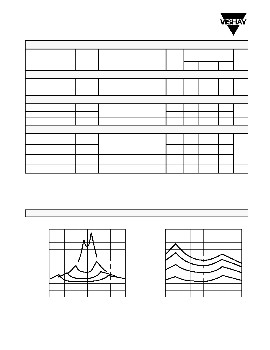
TYPICAL CHARACTERISTICS (25_C UNLESS NOTED)
85
_
C
≠20 ≠16 ≠12
≠8
≠4
0
4
8
12
16
20
40
50
60
70
80
90
100
110
0
10
20
30
40
50
≠15
≠10
≠5
0
5
10
15
"
5 V
r
DS(on)
vs. V
D
and Power Supply Voltages
V
D
≠ Drain Voltage (V)
"
10 V
"
15 V
"
20 V
r
DS(on)
vs. V
D
and Temperature
V
D
≠ Drain Voltage (V)
125
_
C
25
_
C
≠55
_
C
V+ = 15 V
V≠ = ≠15 V
30
20
10
60
70
80
90
100
r DS(on)
≠ Drain-Source On-Resistance (
)
W
r DS(on)
≠ Drain-Source On-Resistance (
)
W

DG211B/212B
Vishay Siliconix
Document Number: 70040
S-00788--Rev. H, 24-Apr-00
www.vishay.com
S
FaxBack 408-970-5600
4-5
TYPICAL CHARACTERISTICS (25_C UNLESS NOTED)
0
2
4
6
8
10
12
14
16
0
25
50
75
100
125
150
175
200
225
r
DS(on)
vs. V
D
and Single Power Supply Voltages
V
D
≠ Drain Voltage (V)
V+ = 5 V
7 V
10 V
12 V
15 V
250
≠20
≠15
≠10
≠5
0
5
10
15
20
40
20
0
≠20
≠40
Leakage Currents vs. Analog Voltage
I
S,
I
D
≠ Current (pA)
I
S(off)
, I
D(off)
I
D(on)
≠55
25
45
5
≠15
65
1 nA
100 pA
10 pA
≠35
1 pA
85
105 125
V+ = 15 V
V≠ = ≠15 V
V
S,
V
D
=
"
14 V
I
S(off)
, I
D(off)
I
S,
I
D
≠ Current
Temperature (
_
C)
Leakage Current vs. Temperature
r DS(on)
≠ Drain-Source On-Resistance (
)
W
V
ANALOG
≠ Analog Voltage (V)
V+ = 22 V
V≠ = ≠22 V
T
A
= 25
_
C
30
10
≠10
≠30
≠15
≠10
≠5
0
5
10
15
30
20
10
0
≠10
≠20
≠30
V+ = 15 V
V≠ = ≠15 V
V+ = 12 V
V≠ = 0 V
Q ≠ Charge (pC)
Q
S,
Q
D
≠ Charge Injection vs. Analog Voltage
V
ANALOG
≠ Analog Voltage (V)
OIRR (dB)
10 k
100 k
1 M
10 M
40
50
60
70
80
90
100
110
120
f ≠ Frequency (Hz)
Off Isolation vs. Frequency
V+ = +15 V
V≠ = ≠15 V
R
L
= 50
W