NO2
COM2
IN2
1
2
3
10
9
Top View
V+
NO1
COM1
8
DG2535
NC2
GND
4
5
7
IN1
NC1
6
NC2
COM2
IN2
1
2
3
10
9
Top View
V+
NC1
COM1
8
DG2536
NO2
GND
4
5
7
IN1
NO1
6
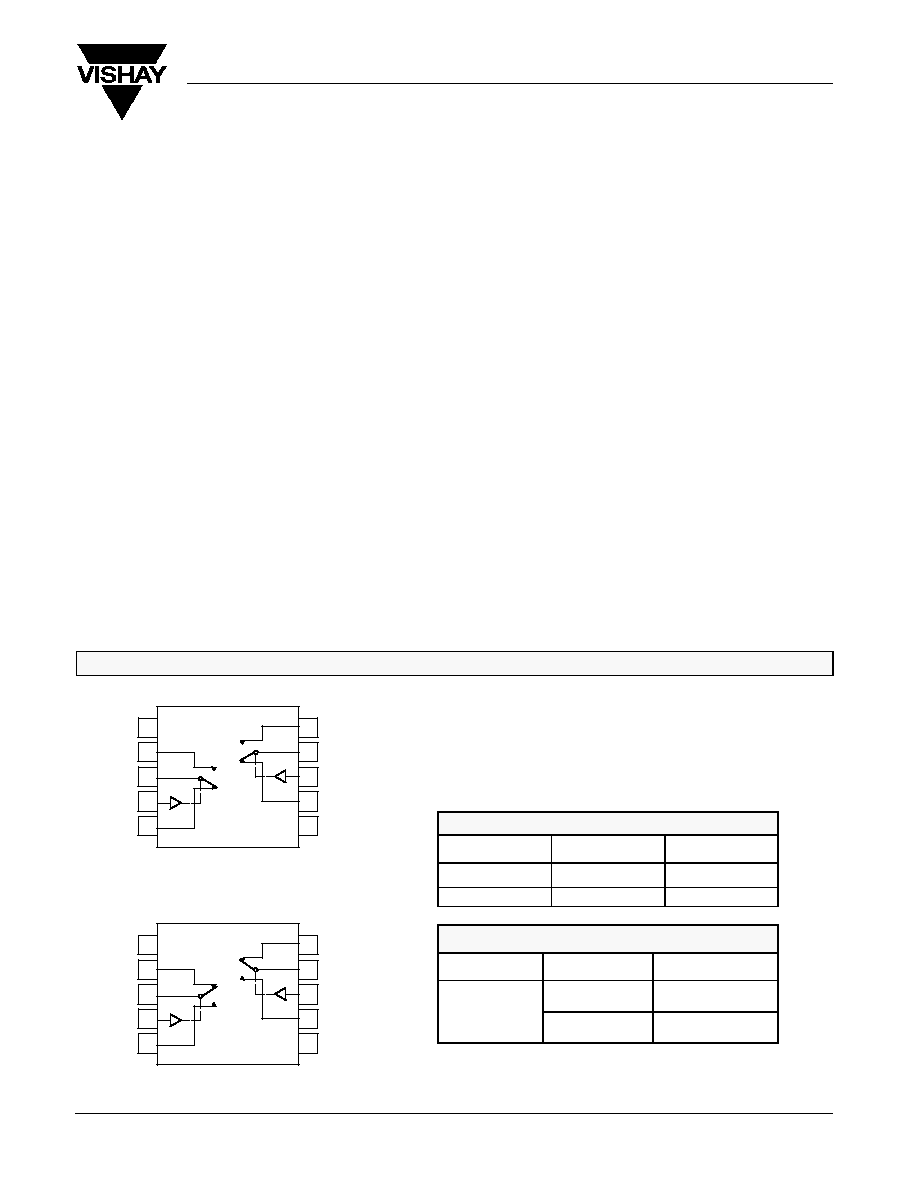
DG2535/DG2536
Vishay Siliconix
New Product
Document Number: 72939
S-41967--Rev. B, 01-Nov-04
www.vishay.com
1
0.35-
W
Low-Voltage Dual SPDT Analog Switch
FEATURES
D Low Voltage Operation
D Low On-Resistance - r
ON:
0.35 W @ 2.7 V
D -69 dB OIRR @ 2.7 V, 100 kHz
D MSOP-10 and DFN-10 Packages
D ESD Protection >2000 V
D Latch-Up Current >300 mA (JESD 78)
BENEFITS
D Reduced Power Consumption
D High Accuracy
D Reduce Board Space
D 1.8-V Logic Compatible
D High Bandwidth
APPLICATIONS
D Cellular Phones
D Speaker Headset Switching
D Audio and Video Signal Routing
D PCMCIA Cards
D Battery Operated Systems
D Relay Replacement
DESCRIPTION
The DG2535/DG2536 is a sub 1-W (0.35 W @ 2.7 V ) dual
SPDT analog switches designed for low voltage applications.
The DG2535/DG2536 has on-resistance matching (less than
0.05 W @ 2.7 V) and flatness (less than 0.2 W @ 2.7 V) that are
guaranteed over the entire voltage range. Additionally, low
logic thresholds make the DG2535/DG2536 an ideal interface
to low voltage DSP control signals.
The DG2535/DG2536 has fast switching speed with
break-before-make guaranteed. In the On condition, all
switching elements conduct equally in both directions.
Off-isolation and crosstalk is -69 dB @ 100 kHz.
The DG2535/DG2536 is built on Vishay Siliconix's
high-density low voltage CMOS process. An eptiaxial layer is
built in to prevent latchup. The DG2535/DG2536 contains the
additional benefit of 2,000-V ESD protection.
In space saving MSOP-10 and DFN-10 lead (Pb)-free packages,
the DG2535/DG2536 are high performance, low r
ON
switches for
battery powered applications. No lead (Pb) is used in the
manufacturing process either inside the device/package or on the
external terminations. As a committed partner to the community
and the environment, Vishay Siliconix manufactures this product
with the lead (Pb)-free device terminations. For analog switching
products manufactured in DFN packages, the lead (Pb)-free
"-E3/E4" suffix is being used as a designator. Lead (Pb)-free
DFN products purchased at any time will have either a
nickel-palladium-gold device termination or a 100% matte tin
device termination. The different lead (Pb)-free materials are
interchangeable and meet all JEDEC standards for reflow and
MSL rating.
FUNCTIONAL BLOCK DIAGRAM AND PIN CONFIGURATION
TRUTH TABLE
Logic
NC1 and NC2
NO1 and NO2
0
ON
OFF
1
OFF
ON
ORDERING INFORMATION
Temp Range
Package
Part Number
40 to 85�C
MSOP-10
DG2535DQ-T1--E3
DG2536DQ-T1--E3
-40 to 85�C
DFN-10
DG2535DN-T1--E3/E4
DG2536DN-T1--E3/E4
DG2535/DG2536
Vishay Siliconix
New Product
www.vishay.com
2
Document Number: 72939
S-41967--Rev. B, 01-Nov-04
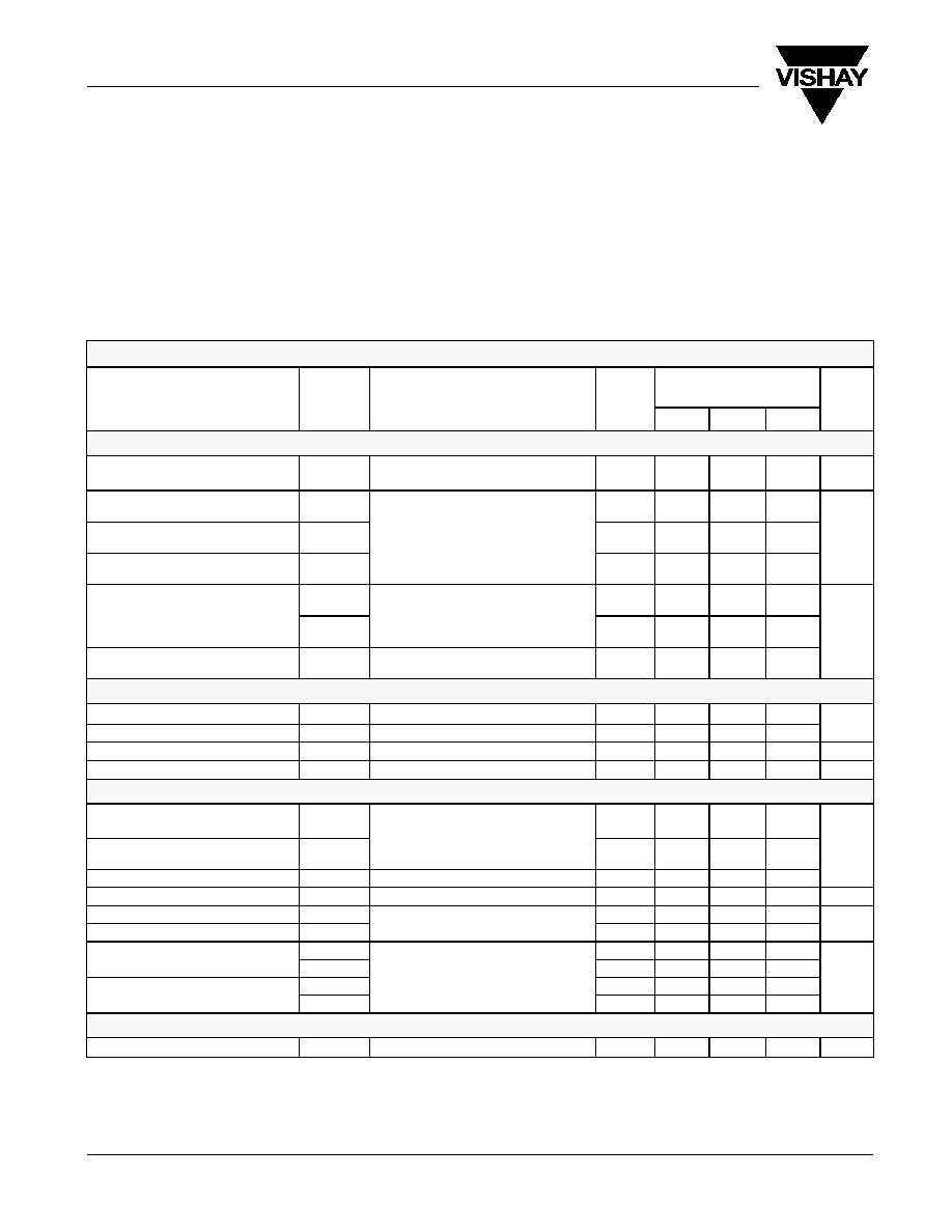
ABSOLUTE MAXIMUM RATINGS
Reference to GND
V+
-0.3 to +6 V
. . . . . . . . . . . . . . . . . . . . . . . . . . . . . . . . . . . . . . . . . . . . . . . . . . . .
IN, COM, NC, NO
a
-0.3 to (V+ + 0.3 V)
. . . . . . . . . . . . . . . . . . . . . . . . . . . . . . . . . . . . . . .
Continuous Current (NO, NC, COM)
"300 mA
. . . . . . . . . . . . . . . . . . . . . . .
Peak Current
"500 mA
. . . . . . . . . . . . . . . . . . . . . . . . . . . . . . . . . . . . . . . . . . . .
(Pulsed at 1 ms, 10% duty cycle)
Storage Temperature (D Suffix)
-65 to 150�C
. . . . . . . . . . . . . . . . . . . . . . . . . .
ESD per Method 3015.7
>2 kV
. . . . . . . . . . . . . . . . . . . . . . . . . . . . . . . . . . . . . . . . . . . . . . .
Power Dissipation (Packages)
b
MSOP-10
c
320 mW
. . . . . . . . . . . . . . . . . . . . . . . . . . . . . . . . . . . . . . . . . . . . . . .
DFN-10
d
1191 mW
. . . . . . . . . . . . . . . . . . . . . . . . . . . . . . . . . . . . . . . . . . . . . . .
Notes:
a.
Signals on NC, NO, or COM or IN exceeding V+ will be clamped by inter-
nal diodes. Limit forward diode current to maximum current ratings.
b.
All leads welded or soldered to PC Board.
c.
Derate 4.0 mW/_C above 70_C
d.
Derate 14.9 mW/_C above 70_C
Stresses beyond those listed under "Absolute Maximum Ratings" may cause permanent damage to the device. These are stress ratings only, and functional operation
of the device at these or any other conditions beyond those indicated in the operational sections of the specifications is not implied. Exposure to absolute maximum rating
conditions for extended periods may affect device reliability.
SPECIFICATIONS (V+ = 3 V)
Test Conditions
Otherwise Unless Specified
Limits
-40 to 85_C
Parameter
Symbol
V+ = 3 V, "10%, V
IN
= 0.5 or 1.4 V
e
Temp
a
Min
b
Typ
c
Max
b
Unit
Analog Switch
Analog Signal Range
d
V
NO
, V
NC
,
V
COM
Full
0
V+
V
On-Resistance
r
ON
V 2 7 V V
0 6/1 5 V
Room
Full
0.35
0.5
0.6
r
ON
Flatness
d
r
ON
Flatness
V+ = 2.7 V, V
COM
= 0.6/1.5 V
I
NO
, I
NC
= 100 mA
Room
0.09
0.2
W
On-Resistance
Match Between Channels
d
Dr
DS(on)
Room
0.05
Switch Off Leakage Current
I
NO(off)
,
I
NC(off)
V+ = 3.3 V, V
NO
, V
NC
= 0.3 V/3 V
Room
Full
-1
-10
1
10
Switch Off Leakage Current
I
COM(off)
V+ = 3.3 V, V
NO
, V
NC
= 0.3 V/3 V
V
COM
= 3 V/0.3 V
Room
Full
-1
-10
1
10
nA
Channel-On Leakage Current
I
COM(on)
V+ = 3.3 V, V
NO
, V
NC
= V
COM
= 0.3 V/3 V
Room
Full
-1
-10
1
10
Digital Control
Input High Voltage
d
V
INH
Full
1.4
V
Input Low Voltage
V
INL
Full
0.5
V
Input Capacitance
C
in
Full
10
pF
Input Current
I
INL
or I
INH
V
IN
= 0 or V+
Full
1
1
mA
Dynamic Characteristics
Turn-On Time
t
ON
V
NO
or V
NC
= 2 0 V R
L
= 50 W C
L
= 35 pF
Room
Full
52
82
90
Turn-Off Time
t
OFF
V
NO
or V
NC
= 2.0 V, R
L
= 50 W, C
L
= 35 pF
Room
Full
43
73
78
ns
Break-Before-Make Time
t
d
V
NO
or V
NC
= 2.0 V, R
L
= 50 W, C
L
= 35 pF
Full
1
6
Charge Injection
d
Q
INJ
C
L
= 1 nF, V
GEN
= 1.5 V, R
GEN
= 0 W
Room
21
pC
Off-Isolation
d
OIRR
R
L
= 50 W C
L
= 5 pF f = 100 KHz
Room
-69
dB
Crosstalk
d
X
TALK
R
L
= 50 W, C
L
= 5 pF, f = 100 KHz
Room
-69
dB
N
O
N
C
Off Capacitance
d
C
NO(off)
Room
145
N
O
, N
C
Off Capacitance
d
C
NC(off)
V
IN
= 0 or V+ f = 1 MHz
Room
145
pF
Channel On Capacitance
d
C
NO(on)
V
IN
= 0 or V+, f = 1 MHz
Room
406
pF
Channel-On Capacitance
d
C
NC(on)
Room
406
Power Supply
Power Supply Current
I+
V
IN
= 0 or V+
Full
1.0
mA
Notes:
a.
Room = 25�C, Full = as determined by the operating suffix.
b.
Typical values are for design aid only, not guaranteed nor subject to production testing.
c.
The algebraic convention whereby the most negative value is a minimum and the most positive a maximum, is used in this data sheet.
d.
Guarantee by design, nor subjected to production test.
e.
V
IN
= input voltage to perform proper function.

DG2535/DG2536
Vishay Siliconix
New Product
Document Number: 72939
S-41967--Rev. B, 01-Nov-04
www.vishay.com
3
TYPICAL CHARACTERISTICS (25_C UNLESS NOTED)
10
10 K
100 K
10 M
100
1 K
1 M
100 mA
10 mA
1 mA
100 mA
10 mA
1 mA
100 nA
1 nA
0.0
0.1
0.2
0.3
0.4
0.5
0.6
0.7
0.8
0.0
0.5
1.0
1.5
2.0
2.5
3.0
0.0
0.1
0.2
0.3
0.4
0.5
0.6
0.7
0.0
0.5
1.0
1.5
2.0
2.5
3.0
3.5
4.0
Supply Current vs. Input Switching Frequency
Input Switching Frequency (Hz)
I+
-
Supply Current (A)
r
ON
vs. V
COM
and Supply Voltage
V
COM
- Analog Voltage (V)
T = 25_C
I
A
= 100 mA
-
On-Resistance (
r
ON
W
)
r
ON
vs. Analog Voltage and Temperature (NC1)
V
COM
- Analog Voltage (V)
-
On-Resistance (
r
ON
W
)
-300
-250
-200
-150
-100
-50
0
50
100
150
200
250
300
0.0
0.5
1.0
1.5
2.0
2.5
3.0
Leakage vs. Analog Voltage
V
COM
- Analog Voltage (V)
V+ = 3 V
10
10000
100000
Supply Current vs. Temperature
Temperature (_C)
100
1000
I+
-
Supply Current (nA)
V+ = 3.0 V
V
IN
= 0 V
-60
-40
-20
0
20
40
60
80
100
1
10000
Leakage Current vs. Temperature
Temperature (_C)
V+ = 3.0 V
100
1000
Leakage Current (pA)
I
COM(on)
I
COM(off)
I
NO(off)
, I
NC(off)
Leakage Current (pA)
V+ = 3.0 V
I
COM(on)
I
COM(off)
I
NO(off)
, I
NC(off)
V+ = 1.8 V
V+ = 2.0 V
V+ = 3.0 V
I
S
= 100 mA
85_C
25_C
-40_C
10 nA
10
V+ = 2.7 V
V+ = 3.0 V
V+ = 3.3 V

DG2535/DG2536
Vishay Siliconix
New Product
www.vishay.com
4
Document Number: 72939
S-41967--Rev. B, 01-Nov-04
TYPICAL CHARACTERISTICS (25_C UNLESS NOTED)
-300
-250
-200
-150
-100
-50
0
50
100
150
200
250
300
0.0
0.5
1.0
1.5
2.0
2.5
3.0
Charge Injection vs. Analog Voltage
V
COM
- Analog Voltage (V)
Q
-
Charge Injection (pC)
0.00
0.25
0.50
0.75
1.00
1.25
1.50
1.75
2.00
0
1
2
3
4
5
6
Switching Threshold vs. Supply Voltage
V+ - Supply Voltage (V)
-
Switching
Threshold (V)
V
T
100 K
-90
10 M
10
-70
-50
100 M
1 G
1 M
Insertion Loss, Off-Isolation
Crosstalk vs. Frequency
Frequency (Hz)
0
10
20
30
40
50
60
70
80
90
100
-60
-40
-20
0
20
40
60
80
100
Switching Time vs. Temperature
/
t
ON
-
Switching
T
ime (ns)
t
OFF
t
ON
V+ = 3 V
t
OFF
V+ = 3 V
(dB)
Loss, OIRR, X
T
ALK
-30
-10
V+ = 3.0 V
OIRR
X
TALK
V+ = 3.0 V
R
L
= 50 W
Temperature (_C)
t
ON
V+ = 2 V
t
OFF
V+ = 2 V
Loss
V+ = 2.0 V
TEST CIRCUITS
FIGURE 1.
Switching Time
Switch
Input
C
L
(includes fixture and stray capacitance)
V+
IN
NO or NC
C
L
35 pF
COM
Logic
Input
R
L
300 W
V
OUT
GND
V+
50%
0 V
Logic
Input
Switch
Output
t
ON
t
OFF
Logic "1" = Switch On
Logic input waveforms inverted for switches that have
the opposite logic sense.
0 V
Switch Output
V
OUT
+ V
COM
R
L
R
L
) R
ON
0.9 x V
OUT
t
r
t 5 ns
t
f
t 5 ns
V
INH
V
INL

DG2535/DG2536
Vishay Siliconix
New Product
Document Number: 72939
S-41967--Rev. B, 01-Nov-04
www.vishay.com
5
TEST CIRCUITS
FIGURE 2.
Break-Before-Make Interval
C
L
= 1 nF
R
gen
V
OUT
COM
V
IN
= 0 - V+
IN
GND
V+
V+
+
NC or NO
FIGURE 3.
Charge Injection
C
L
(includes fixture and stray capacitance)
NC
V
NO
NO
V
NC
0 V
Logic
Input
Switch
Output
V
O
V
NC
= V
NO
90%
t
D
IN
COM
V+
GND
V+
C
L
35 pF
V
O
R
L
300 W
V
INL
V
INH
t
r
t 5 ns
t
f
t 5 ns
t
D
Off
On
On
IN
DV
OUT
V
OUT
Q = DV
OUT
x C
L
IN depends on switch configuration: input polarity
determined by sense of switch.
FIGURE 4.
Off-Isolation
FIGURE 5.
Channel Off/On Capacitance
NC or NO
f = 1 MHz
IN
COM
GND
0 V, 2.4 V
Meter
HP4192A
Impedance
Analyzer
or Equivalent
10 nF
V+
V+
IN
GND
NC or NO
0V, 2.4 V
10 nF
COM
Off Isolation + 20 log
V
COM
V
NO NC
R
L
Analyzer
V+
V+
COM
Vishay Siliconix maintains worldwide manufacturing capability. Products may be manufactured at one of several qualified locations. Reliability data for Silicon Technology and
Package Reliability represent a composite of all qualified locations. For related documents such as package/tape drawings, part marking, and reliability data, see
http://www.vishay.com/ppg?72939
.