 | –≠–ª–µ–∫—Ç—Ä–æ–Ω–Ω—ã–π –∫–æ–º–ø–æ–Ω–µ–Ω—Ç: DG309 | –°–∫–∞—á–∞—Ç—å:  PDF PDF  ZIP ZIP |

IN
1
IN
2
D
1
D
2
S
1
S
2
V≠
V+
GND
NC
S
4
S
3
D
4
D
3
IN
4
IN
3
1
2
3
4
5
6
7
8
16
15
14
13
12
11
10
9
Top View
DG308A
DG308A/DG309
Vishay Siliconix
Document Number: 70046
S-52882--Rev. E, 28-Apr-97
www.vishay.com
S
FaxBack 408-970-5600
4-1
Quad Monolithic SPST CMOS Analog Switches
FEATURES
BENEFITS
APPLICATIONS
D "
15-V Analog Input Range
D
Low On-Resistance: 60
W
D
Fast Switching: 130 ns
D
Low Power Dissipation: 30 nW
D
CMOS Logic Compatible
D
Full Rail-to-Rail Analog Signal Range
D
Low Signal Error
D
Wide Dynamic Range
D
Single or Dual Supply Capability
D
Static Protected Logic Inputs
D
Space Savings (TSSOP)
D
Portable and Battery Powered
Instrumentation
D
Communication Systems
D
Computer Peripherals
D
High-Speed Multiplexing
DESCRIPTION
Featuring low on-resistance (60
W
) and fast switching
(130 ns), the DG308A is supplied in the "normally open"
configuration while DG309 is supplied "normally closed." Input
thresholds are high voltage CMOS compatible.
Designed with the Vishay Siliconix PLUS-40 CMOS process
to combine low power dissipation with a high breakdown
voltage rating of 44 V, each switch conducts equally well in
both directions when on, and blocks up to the supply voltage
when off. An epitaxial layer prevents latch up.
The DG308B/309B upgrades are recommended for new
designs.
FUNCTIONAL BLOCK DIAGRAM AND PIN CONFIGURATION
Four SPST Switches per Package
TRUTH TABLE
Logic
DG308A
DG309
0
OFF
ON
1
ON
OFF
Logic "0"
v
3.5 V
Logic "1"
w
11 V

DG308A/DG309
Vishay Siliconix
www.vishay.com
S
FaxBack 408-970-5600
4-2
Document Number: 70046
S-52882--Rev. E, 28-Apr-97
ORDERING INFORMATION
Temp Range
Package
Part Number
0 to 70
_
C
16-Pin Plastic DIP
DG308ACJ
0 to 70
_
C
16-Pin Plastic DIP
DG309CJ
40
85 C
16-Pin Narrow SOIC
DG308ADY
≠40 to 85
_
C
16-Pin Narrow SOIC
DG309DY
≠40 to 85
_
C
16-Pin TSSOP
DG308ADQ
16-Pin TSSOP
DG309DQ
≠55 to 125
_
C
16-Pin CerDIP
DG308AAK/883
≠55 to 125
_
C
16-Pin CerDIP
DG309AK/883
ABSOLUTE MAXIMUM RATINGS
Voltages Referenced to V≠
V+
44 V
. . . . . . . . . . . . . . . . . . . . . . . . . . . . . . . . . . . . . . . . . . . . . . . . . . . . . . . . . . .
GND
25 V
. . . . . . . . . . . . . . . . . . . . . . . . . . . . . . . . . . . . . . . . . . . . . . . . . . . . . . . . .
Digital Inputs
a
, V
S
, V
D
(V≠) ≠2 V to (V+) +2V or
. . . . . . . . . . . . . . . . . . . . . . . . .
20 mA, whichever occurs first
Current, Any Terminal Except S or D
30 mA
. . . . . . . . . . . . . . . . . . . . . . . . . . .
Continuous Current, S or D
20 mA
. . . . . . . . . . . . . . . . . . . . . . . . . . . . . . . . . . .
(Pulsed at 1 ms, 10% duty cycle max)
70 mA
. . . . . . . . . . . . . . . . . . . . . . . . . .
Storage Temperature
(AK Suffix)
≠65 to 150
_
C
. . . . . . . . . . . . . . . . . .
(CJ, DY, and DQ Suffix)
≠65 to 125
_
C
. . . . . . .
Power Dissipationb
16-Pin Plastic DIP
c
470 mW
. . . . . . . . . . . . . . . . . . . . . . . . . . . . . . . . . . . . . . . . .
16-Pin Narrow SOIC and TSSOP
e
600 mW
. . . . . . . . . . . . . . . . . . . . . . . . . . . .
16-Pin Cerdip
d
900 mW
. . . . . . . . . . . . . . . . . . . . . . . . . . . . . . . . . . . . . . . . . . . . .
Notes:
a.
Signals on S
X
, D
X
, or IN
X
exceeding V+ or V≠ will be clamped by internal
diodes. Limit forward diode current to maximum current ratings.
b.
All leads welded or soldered to PC Board.
c.
Derate 12 mW/
_
C above 75
_
C
d.
Derate 6.5 mW/
_
C above 25
_
C
e.
Derate 7.6 mW/
_
C above 75
_
C
SCHEMATIC DIAGRAM (TYPICAL CHANNEL)
FIGURE 1.
Level
Shift/
Drive
V
IN
S
V+
GND
V≠
D
V≠
V+

DG308A/DG309
Vishay Siliconix
Document Number: 70046
S-52882--Rev. E, 28-Apr-97
www.vishay.com
S
FaxBack 408-970-5600
4-3
SPECIFICATIONS
a
Test Conditions
Unless Otherwise Specified
A Suffix
≠55 to 125
_
C
C, D Suffix
Parameter
Symbol
V+ = 15 V, V≠ = ≠15 V
V
IN
= 3.5 V or 11 V
f
Temp
b
Typ
c
Min
d
Max
d
Min
d
Max
d
Unit
Analog Switch
Analog Signal Range
e
V
ANALOG
Full
≠15
15
≠15
15
V
Drain-Source
On-Resistance
r
DS(on)
V
D
=
"
10 V, I
S
= 1 mA
Room
Full
60
100
150
100
125
W
Source Off
Leakage Current
I
S(off)
V
S
=
"
14 V, V
D
=
#
14 V
Room
Full
"
0.1
≠1
≠100
1
100
≠5
≠100
5
100
A
Drain Off
Leakage Current
I
D(off)
V
D
=
"
14 V, V
S
=
#
14 V
Room
Full
"
0.1
≠1
≠100
1
100
≠5
≠100
5
100
nA
Drain On
Leakage Current
I
D(on)
V
D
= V
S
=
"
14 V
Room
Full
"
0.1
≠1
≠100
1
100
≠5
≠200
5
200
Digital Control
Input Current with
Input Voltage High
I
INH
V
IN
= 15 V
Full
0.001
1
1
m
A
Input Current with
Input Voltage Low
I
INL
V
IN
= 0 V
Full
≠0.001
≠1
≠1
m
A
Input Capacitance
C
IN
Room
8
pF
Dynamic Characteristics
Turn-On Time
t
ON
See Figure 2
Room
130
200
200
ns
Turn-Off Time
t
OFF
See Figure 2
Room
90
150
150
ns
Charge Injection
Q
C
L
= 0.01
m
F, R
gen
= 0
W
, V
gen
= 0 V
Room
≠10
pC
Source-Off
Capacitance
C
S(off)
f
140 kH
V
V
0 V
Room
11
F
Drain-Off
Capacitance
C
D(off)
f = 140 kHz, V
S
, V
D
= 0 V
Room
8
pF
Channel-On
Capacitance
C
D(on)
Room
27
Off-Isolation
f
OIRR
R
L
= 75 , V
S
= 2 V
p-p
, f = 500 kHz
Room
78
dB
Power Supplies
Positive
Supply Current
I+
All Channels On or Off
Room
Full
0.001
10
100
10
100
m
A
Negative
Supply Current
I≠
All Channels On or Off
V
IN
= 0 V or 15 V
Room
Full
≠0.001
≠10
≠100
≠100
m
A
Notes:
a.
Refer to PROCESS OPTION FLOWCHART.
b.
Room = 25
_
C, Full = as determined by the operating temperature suffix.
c.
Typical values are for DESIGN AID ONLY, not guaranteed nor subject to production testing.
d.
The algebraic convention whereby the most negative value is a minimum and the most positive a maximum, is used in this data sheet.
e.
Guaranteed by design, not subject to production test.
f.
V
IN
= input voltage to perform proper function.
DG308A/DG309
Vishay Siliconix
www.vishay.com
S
FaxBack 408-970-5600
4-4
Document Number: 70046
S-52882--Rev. E, 28-Apr-97
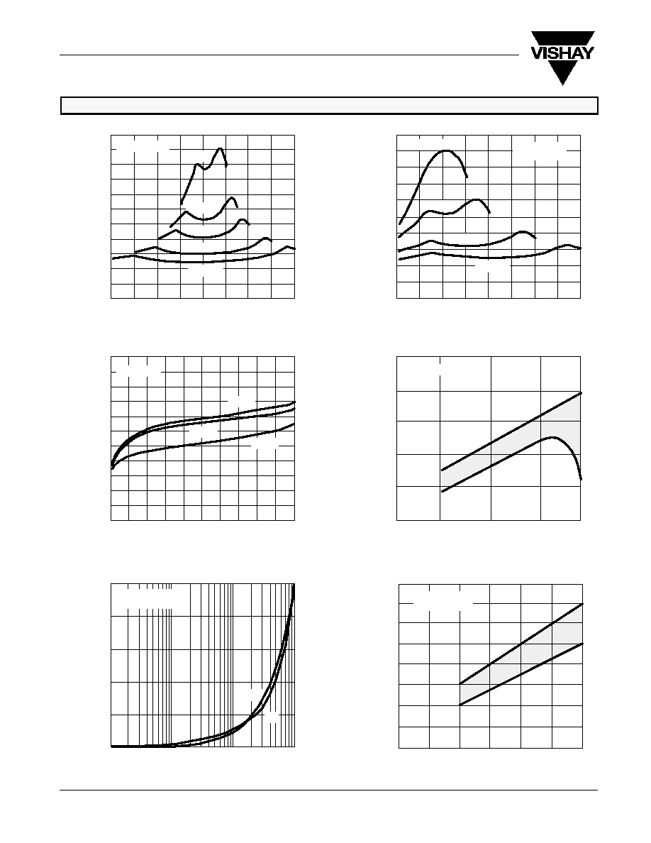
TYPICAL CHARACTERISTICS (25_C UNLESS NOTED)
r DS(on)
≠ Drain-Source On-Resistance (
)
W
≠12
≠6
0
6
12
15
9
3
≠3
≠9
≠15
150
≠10
0
10
20
120
90
60
30
0
T
A
= 25
_
C
r
DS(on)
vs. V
D
and Power Supply
15
5
≠5
≠15
250
0
5
10
15
20
200
150
100
50
0
r
DS(on)
vs. V
D
and Power Supply Voltage
T
A
= 25
_
C
V≠ = 0 V
10
0
≠10
≠20
≠30
Leakage Currents vs. Analog Voltage
(pA)
I
, I
SD
T
A
= 25
_
C
10
0
8
6
4
2
Input Switching Threshold
vs. V+ and V≠ Supply Voltages
V+, V≠ Positive & Negative Supplies (V)
(V)
T
V
T
A
= 25
_
C
0
"
5
"
10
"
15
"
20
r DS(on)
≠ Drain-Source On-Resistance (
)
W
"
5 V
"
7.5 V
"
10 V
"
15 V
"
20 V
+10 V
+15 V
+20 V
V+ = +7.5 V
V
D
≠ Drain Voltage (V)
V
D
≠ Drain Voltage (V)
V
D
or V
S
≠ Drain or Source Voltage (V)
I
S(off)
I
D(off)
I
D(on)
1000
800
600
400
200
I +
Supply Currents vs. Switching Frequency
(All Inputs Active)
1 k
10 k
100 k
1 M
"
15 V Supplies
T
A
= 25
_
C
I≠
100
8
0
5
10
15
7
6
5
4
3
2
1
0
Input Switching Threshold vs. Positive
Supply Voltage
V+ ≠ Positive Supply Voltage (V)
V≠ = 0 V
T
A
= 25
_
C
I+, I≠ (
m
A)
(V)
T
V
f ≠ Frequency (Hz)

DG308A/DG309
Vishay Siliconix
Document Number: 70046
S-52882--Rev. E, 28-Apr-97
www.vishay.com
S
FaxBack 408-970-5600
4-5
TEST CIRCUITS
FIGURE 2. Switching Time
50%
0 V
12 V
t
OFF
t
ON
V
O
t
r
<20 ns
t
f
<20 ns
Logic
Input
Switch
Output
90%
C
L
35 pF
R
L
1 k
W
V
O
= V
S
R
L
+ r
DS(on)
R
L
V
S
= +3 V
V
O
V≠
V+
IN
S
D
12 V
≠15 V
GND
+15 V
APPLICATIONS
Single Supply Operation
The DG308A and DG309 will switch positive analog signals
while using a single positive supply. This will allow use in many
applications where only one supply is available. The trade-offs
or performance given up while using single supplies are:
1) increased r
DS(on)
and 2) slower switching speed. As stated
in the absolute maximum ratings section of the data sheet, the
analog voltage should not go above or below the supply
voltages which in single supply operation are V+ and 0 V.