 | ÐлекÑÑоннÑй компоненÑ: DG3157 | СкаÑаÑÑ:  PDF PDF  ZIP ZIP |
Äîêóìåíòàöèÿ è îïèñàíèÿ www.docs.chipfind.ru

S
A
1
2
3
6
Top View
B
1
GND
B
0
4
SC-70
6- Pin
Device Marking: G1
5
V+
DG3157
Vishay Siliconix
New Product
Document Number: 72648
S-32552--Rev. A, 15-Dec-03
www.vishay.com
1
High-Speed, Low r
ON
, SPDT Analog Switch
(2:1 Multiplexer/Demultiplexer Bus Switch)
FEATURES
D Direct Cross to Industry Standard SN74LVC1G3157
NC7SB3157, NLASB3175, Pl5A3157, and STG3157
D SC-70 6-Lead Package
D 1.65-V to 5.5-V V
CC
Operation
D 5-W Connection Between Ports
D Minimal Propagation Delay
D Break-Before-Make Switching
D Zero Bounce In Flow-Through Mode
DESCRIPTION
The DG3157 is a high-speed single-pole double-throw, low
power, TTL-Compatible bus switch. Using sub-micro CMOS
technology, the DG3157 achieves low on-resistance and
negligible propagation delay.
The DG3157 can handle both analog and digital signals and
permits signals with amplitudes of up to V
CC
to be transmitted
in either direction.
When the Select pin is low, B
0
is connected to the output A pin.
When the Select pin is high, B
1
is connected to the output A
pin. The path that is open will have a high-impedance state
with respect to the output. Make-before-break is guaranteed.
An eptiaxial layer prevents latch-up.
FUNCTIONAL BLOCK DIAGRAM AND PIN CONFIGURATION
TRUTH TABLE
Logic Input (S)
Function
0
B
0
Connected to A
1
B
1
Connected to A
ORDERING INFORMATION
Temp Range
Package
Part Number
-40 to 85°C
SC70-6
DG3157DL
DG3157
Vishay Siliconix
New Product
www.vishay.com
2
Document Number: 72648
S-32552--Rev. A, 15-Dec-03
ABSOLUTE MAXIMUM RATINGS
Reference to GND
V+
-0.3 to +6 V
. . . . . . . . . . . . . . . . . . . . . . . . . . . . . . . . . . . . . . . . . . . . . . . . . . . .
S, A, B
a
-0.3 to (V+ + 0.3 V)
. . . . . . . . . . . . . . . . . . . . . . . . . . . . . . . . . . . . . . . . . . . . . . . . . .
Continuous Current (Any terminal)
"50 mA
. . . . . . . . . . . . . . . . . . . . . . . . . . .
Peak Current
"200 mA
. . . . . . . . . . . . . . . . . . . . . . . . . . . . . . . . . . . . . . . . . . . . .
(Pulsed at 1 ms, 10% duty cycle)
Storage Temperature (D Suffix)
-65 to 150°C
. . . . . . . . . . . . . . . . . . . . . . . . . . . .
Power Dissipation (Packages)
b
6-Pin SC70
c
250 mW
. . . . . . . . . . . . . . . . . . . . . . . . . . . . . . . . . . . . . . . . . . . . . . .
Notes:
a.
Signals on A, or B or S exceeding V+ will be clamped by internal diodes.
Limit forward diode current to maximum current ratings.
b.
All leads welded or soldered to PC Board.
c.
Derate 3.1 mW/_C above 70_C
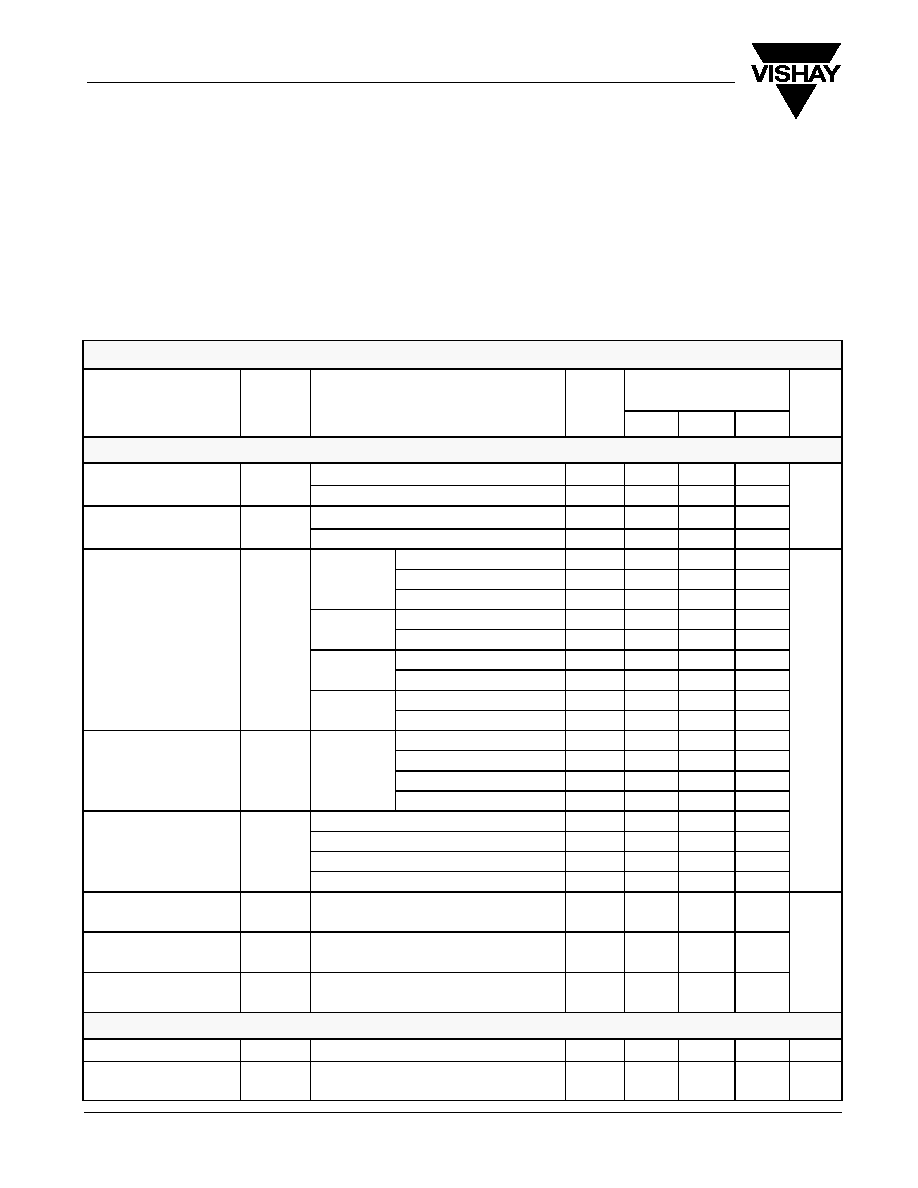
SPECIFICATIONS
Test Conditions
Otherwise Unless Specified
Limits
-40 to 85_C
Parameter
Symbol
V+ = 3.0 V, V
S
= 0.25 V to 0.7 V+
e
Temp
a
Min
b
Typ
c
Max
b
Unit
DC Characteristics
High Level Input Voltage
V
SH
V+ = 1.65 to 1.95 V
Full
0.75 V+
High Level Input Voltage
V
SH
V+ = 2.3 to 5.5 V
Full
0.7 V+
V
Low Level Input Voltage
V
SL
V+ = 1.65 to 1.95 V
Full
0.25 V+
V
Low Level Input Voltage
V
SL
V+ = 2.3 to 5.5 V
Full
0.3 V+
VBN = 0 V, I
A
= 30 mA
Full
6
7
V+ = 4.5 V
VBN = 2.3 V, I
A
= -30 mA
Full
6
12
VBN = 4.5 V, I
A
= -30 mA
Full
9
15
V+ = 3 0 V
VBN = 0 V, I
A
= 24 mA
Full
8
9
On Resistance
R
ON
V+ = 3.0 V
VBN = 3.0 V, I
A
= -24 mA
Full
12
20
ON
V+ = 2 3 V
VBN = 0 V, I
A
= 8 mA
Full
9
12
V+ = 2.3 V
VBN = 2.3 V, I
A
= -8 mA
Full
13
30
V+ = 1 65 V
VBN = 0 V, I
A
= 4 mA
Full
12
20
V+ = 1.65 V
VBN = 1.8 V, I
A
= -4 mA
Full
18
50
W
V+ = 4.5 V, I
A
= -30 mA
Room
6
On Resistance Fltaness
R
FLAT
0 < V
BN
< V+
V+ = 3.0 V, I
A
= -24 mA
Room
12
On Resistance Fltaness
R
FLAT
0 < V
BN
< V+
V+ = 2.3 V, I
Z
= -8 mA
Room
22
V+ = 1.65 V, I
A
= -4 mA
Room
90
V+ = 4.5 V, V
BN
= 3.15 V, I
A
= -30 mA
Room
0.32
On Resistance Matching
DR
ON
V+ = 3.0 V, V
BN
= 2.1 V, I
A
= -24 mA
Room
0.31
On Resistance Matching
Between Channels
DR
ON
V+ = 2.3 V, V
BN
= 1.6 V, I
A
= -8 mA
Room
0.30
V+ = 1.65 V, V
BN
= 1.15 V, I
A
= -4 mA
Room
0.29
Input Leakage Current
I
S
V+ = 5 5 V V
A
= 5 5 V
Room
-0.1
0.1
Input Leakage Current
I
S
V+ = 5.5 V, V
A
= 5.5 V
Full
-1.0
-1.0
Off Stage Switch Leakage
I
BN( ff)
V+ = 5 5 V V
A
/V
B
= 0 V/5 5 V
Room
-0.1
0.1
mA
Off Stage Switch Leakage
I
BN(off)
V+ = 5.5 V, V
A
/V
B
= 0 V/5.5 V
Full
-1.0
-1.0
mA
On State Switch Leakage
I
BN( )
V+ = 5 5 V V
A
/V
B
= 0 V/5 5 V
Room
-0.1
0.1
On State Switch Leakage
I
BN(on)
V+ = 5.5 V, V
A
/V
B
= 0 V/5.5 V
Full
-1.0
-1.0
Power Supply
Power Supply Range
V+
Full
1.8
5.5
Quiescent Supply Current
I+
V+ = 5 5 V V
A
= V
B
= V+ or GND
Room
1
mA
Quiescent Supply Current
I+
V+ = 5.5 V, V
A
= V
B
= V+ or GND
Full
10
mA

DG3157
Vishay Siliconix
New Product
Document Number: 72648
S-32552--Rev. A, 15-Dec-03
www.vishay.com
3
SPECIFICATIONS
Parameter
Limits
-40 to 85_C
Temp
a
Test Conditions
Otherwise Unless Specified
Symbol
Parameter
Unit
Max
b
Typ
c
Min
b
Temp
a
V+ = 3.0 V, V
S
= 0.25 V to 0.7 V+
e
Symbol
AC Electrical Characteristice
V+ =1.65 to 1.95 V
Full
Prop Delay Time
f
t
PHL
/t
PLH
V
A
= 0 V
V+ =2.3 to 2.7 V
Full
1.2
Prop Delay Time
f
t
PHL
/t
PLH
V
A
= 0 V
V+ =3.0 to 3.6 V
Full
0.8
V+ =4.5 to 5.5 V
Full
0.3
V+ =1 65 to 1 95 V
Room
10.2
V+ =1.65 to 1.95 V
Full
10.4
V+ =2 3 to 2 7 V
Room
5.9
Output Enable Time
f
t
PZL
/t
PZH
V
LOAD
= 2 x V+ for t
PZL
V+ =2.3 to 2.7 V
Full
6.2
Output Enable Time
f
t
PZL
/t
PZH
V
LOAD
= 2 x V+ for t
PZL
V
LOAD
= 0 V for t
PZH
V+ =3 0 to 3 6 V
Room
4.1
V+ =3.0 to 3.6 V
Full
4.5
V+ =4 5 to 5 5 V
Room
2.6
V+ =4.5 to 5.5 V
Full
2.9
ns
V+ =1 65 to 1 95 V
Room
10.2
ns
V+ =1.65 to 1.95 V
Full
10.4
V+ =2 3 to 2 7 V
Room
5.9
Output Disable Time
f
t
PLZ
/t
PHZ
V
LOAD
= 2 x V+ for t
PLZ
V+ =2.3 to 2.7 V
Full
6.2
Output Disable Time
f
t
PLZ
/t
PHZ
V
LOAD
= 2 x V+ for t
PLZ
V
LOAD
= 0 V for t
PHZ
V+ =3 0 to 3 6 V
Room
4.1
V+ =3.0 to 3.6 V
Full
4.5
V+ =4 5 to 5 5 V
Room
2.6
V+ =4.5 to 5.5 V
Full
2.9
V+ =1.65 to 1.95 V
Full
0.5
Break Before Make Time
d
t
BBM
V+ =2.3 to 2.7 V
Full
0.5
Break-Before-Make Time
d
t
BBM
V+ =3.0 to 3.65 V
Full
0.5
V+ =4.5 to 5.5 V
Full
0.5
Charge Injection
d
Q
C
L
= 0.1 nF, V
GEN
= 0 V
V+ = 5 V
Room
7
pC
Charge Injection
d
Q
C
L
= 0.1 nF, V
GEN
= 0 V
R
GEN
= 0 W
V+ = 3.3 V
Room
3
pC
Analog Switch Characteristics
Off Isolation
d
OIRR
R
L
= 50 W f = 10 MHz
Room
-57.6
dB
Crosstalk
d
X
TALK
R
L
= 50 W, f = 10 MHz
Room
-58.7
dB
-3-db Bandwidth
d
BW
R
L
= 50 W
Room
u250
MHz
Capacitance
Control Pin Capacitance
d
C
IN
V+ = 0 V
Room
4.9
pF
B Port Off Capacitance
d
C
IO-B
Room
t6.5
pF
A Port Capacitance When
Switch Enable
d
C
IO-A(on)
V+ = 5 V
Room
t18.5
Notes:
a.
Room = 25°C, Full = as determined by the operating suffix.
b.
The algebraic convention whereby the most negative value is a minimum and the most positive a maximum, is used in this data sheet.
c.
Typical values are for design aid only, not guaranteed nor subject to production testing.
d.
Guarantee by design, nor subjected to production test.
e.
V
IN
= input voltage to perform proper function.
f.
Guaranteed by design and not production tested. The bus switch propagation delay is a function of the RC time constant contributed by the on-resistance and
the specified load capacitance with an ideal voltage source (zero output impedance) driving the switch.

DG3157
Vishay Siliconix
New Product
www.vishay.com
4
Document Number: 72648
S-32552--Rev. A, 15-Dec-03
LOGIC DIAGRAM (POSITIVE LOGIC)
Figure 1.
A
B
B
S
4
1
6
3
TYPICAL CHARACTERISTICS (25_C UNLESS NOTED)
0
5
10
15
20
25
30
35
40
0.0
0.5
1.0
1.5
2.0
2.5
3.0
3.5
4.0
4.5
r
ON
vs. V
A
vs. V
CC
V
A
(V)
V+ = 1.65 V, I
S
= 4 mA
r
ON
-
On Resistance (
W
)
V+ = 2.3 V, I
S
= 8 mA
V+ = 3.0 V, I
S
= 24 mA
V+ = 4.5 V, I
S
= 30 mA

DG3157
Vishay Siliconix
New Product
Document Number: 72648
S-32552--Rev. A, 15-Dec-03
www.vishay.com
5
AC LOADING AND WAVEFORMS
t
r
= 2.5 ns
t
f
= 2.5 ns
t
f
= 2.5 ns
t
r
= 2.5 ns
3.0 V
3.0 V
GND
GND
Logic
Input
Switch
Input
10%
10%
10%
10%
1.5 V
1.5 V
1.5 V
1.5 V
1.5 V
1.5 V
1.5 V
90%
90%
90%
90%
t
w
Output
Output
Output
t
PLH
t
PHL
V
OH
V
OL
t
PZL
t
PLZ
t
PZH
t
PHZ
1.5 V
V
OL
+ 0.3 V
V
OL
V
OH
V
OH
-0.3 V
V
LD
2
0 V
From Output
Under Test
V
LD
R
L
500 W
C
L
50 pF
Load Circuit
Figure 2. AC Test Circuit
Figure 3. AC Waveforms
R
L
500 W
Open
GND
SW
t
PLH
/t
PHL
Open
t
PLZ
/t
PZL
V
LD
t
PHZ
/t
PZH
GND
TEST
SW
Waveform 1
SW at V
LD
Waveform 2
SW at GND
Propagation Delay Times
Enable and Disable Time--Low- and High-Level Enabling
Notes:
a.
C
L
includes probe and jig capacitance.
b.
Waveform 1 is for an output with internal conditions such that the output is low except when disabled by the output control.
c.
Waveform 2 is for an output with internal conditions such that the output is high except when disabled by the output control.
d.
All input pulses are supplied by generators having the following characteristics: PRR v 10 MHz, Z
O
= 50 W.
e.
The outputs are measured one at a time with one transition per measurement.
f.
t
PLZ
and t
PHZ
are the same as t
dis
.
g.
t
PZL
and t
PZH
are the same as t
dis
.
h.
t
PLH
and t
PHL
are the same as t
dis
.
i.
V
LD
= 2 V+.