1
2
3
4
5
6
7
8
16
15
14
13
12
11
10
9
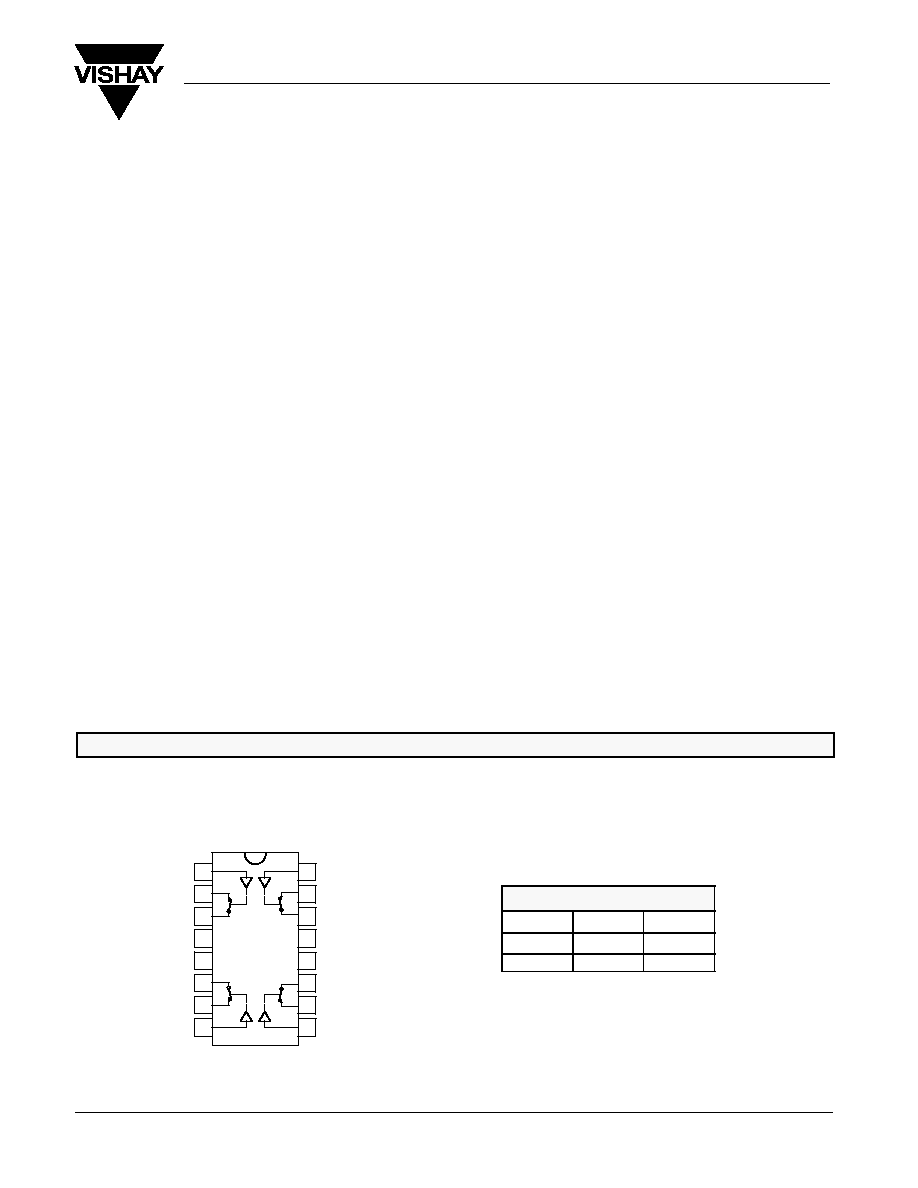
Top View
IN
1
IN
2
D
1
D
2
S
1
S
2
V-
V+
GND
V
L
S
4
S
3
D
4
D
3
IN
4
IN
3
TSSOP and SOIC
DG411L/412L
DG411L/412L/413L
Vishay Siliconix
Document Number: 71397
S-21452--Rev. C, 26-Aug-02
www.vishay.com
1
Precision Monolithic Quad SPST
Low-Voltage CMOS Analog Switches
FEATURES
BENEFITS
APPLICATIONS
D
2.7- thru 12-V Single Supply or
"
3- thru
"
6-Dual Supply
D
On-Resistance--r
DS(on)
: 17
W
D
Fast Switching--t
ON
: 19 ns
--t
OFF
: 12 ns
D
TTL, CMOS Compatible
D
Low Leakage: 0.25 nA
D
2000-V ESD Protection
D
Widest Dynamic Range
D
Low Signal Errors and Distortion
D
Break-Before-Make Switching Action
D
Simple Interfacing
D
Precision Automatic Test Equipment
D
Precision Data Acquisition
D
Communication Systems
D
Battery Powered Systems
D
Computer Peripherals
D
SDSL, DSLAM
D
Audio and Video Signal Routing
DESCRIPTION
The DG411L/412L/413L are low voltage pin-for-pin
compatible companion devices to the industry standard
DG411/412/413 with improved performance
Using BiCMOS wafer fabrication technology allows the
DG411L/412L/413L to operate on single and dual supplies.
Single supply voltage ranges from 3 to 12 V while dual supply
operation is recommended with
"
3 to
"
6 V.
Combining high speed (t
ON
: 19 ns), flat r
DS(on)
over the analog
signal range (5
W
), minimal insertion lose (-3 dB at 280 MHz),
and excellent crosstalk and off-isolation performance (-50 dB
at 50 MHz), the DG411L/412L/413L are ideally suited for audio
and video signal switching.
The DG411L and DG412L respond to opposite control logic as
shown in the Truth Table. The DG413L has two normally open
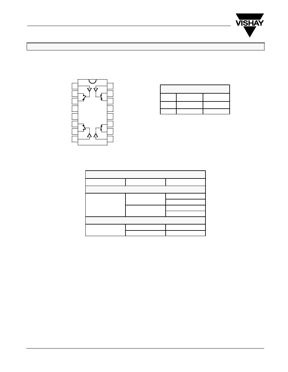
and two normally closed switches.
FUNCTIONAL BLOCK DIAGRAM AND PIN CONFIGURATION
TRUTH TABLE
Logic
DG411L
DG412L
0
ON
OFF
1
OFF
ON
v
Logic "0"
v
0.8 V
w
Logic "1"
w
2.4 V
1
2
3
4
5
6
7
8
16
15
14
13
12
11
10
9
Top View
IN
1
IN
2
D
1
D
2
S
1
S
2
V-
V+
GND
V
L
S
4
S
3
D
4
D
3
IN
4
IN
3
Dual-In-Line and SOIC
DG413L
DG411L/412L/413L
Vishay Siliconix
www.vishay.com
2
Document Number: 71397
S-21452--Rev. C, 26-Aug-02
FUNCTIONAL BLOCK DIAGRAM AND PIN CONFIGURATION
TRUTH TABLE
Logic
SW
1
, SW
4
SW
2
, SW
3
0
OFF
ON
1
ON
OFF
v
Logic "0"
v
0.8 V
w
Logic "1"
w
2.4 V
ORDERING INFORMATION
Temp Range
Package
Part Number
DG411L/412L
DG411LDY
_
16-Pin Narrow SOIC
DG412LDY
-40 to 85
_
C
DG411LDQ
16-Pin TSSOP
DG412LDQ
DG413L
_
16-Pin Narrow SOIC
DG413LDY
-40 to 85
_
C
16-Pin TSSOP
DG413LDQ
ABSOLUTE MAXIMUM RATINGS
V+ to V-
-0.3 TO 13 V
. . . . . . . . . . . . . . . . . . . . . . . . . . . . . . . . . . . . . . . . . . . . . .
GND to V-
7 V
. . . . . . . . . . . . . . . . . . . . . . . . . . . . . . . . . . . . . . . . . . . . . . . . . . . . .
V
L
(GND -0.3 V) to (V+) +0.3 V
. . . . . . . . . . . . . . . . . . . . . . . . . . . . . . . . . . . . . . .
I
N
a
, V
S
, V
D
-0.3 to (V+ +0.3 V) or 30 mA, whichever occurs first
. . . . . . . . . .
Continuous Current (Any Terminal)
30 mA
. . . . . . . . . . . . . . . . . . . . . . . . . . . . .
Peak Current, S or D (Pulsed 1 ms, 10% Duty Cycle)
100 mA
. . . . . . . . . . . .
Storage Temperature
(DQ, DY Suffix)
-65 to 125
_
C
. . . . . . . . . . . . . .
Power Dissipation (Package)
b
16-Pin TSSOP
c
450 mW
. . . . . . . . . . . . . . . . . . . . . . . . . . . . . . . . . . . . . . . . . . . .
16-Pin SOIC
d
650 mW
. . . . . . . . . . . . . . . . . . . . . . . . . . . . . . . . . . . . . . . . . . . . . .
Notes:
a.
Signals on S
X
, D
X
, or IN
X
exceeding V+ or V- will be clamped by internal
diodes. Limit forward diode current to maximum current ratings.
b.
All leads welded or soldered to PC Board.
c.
Derate 7 mW/
_
C above 75
_
C
d.
Derate 7.6 mW/
_
C above 75
_
C

DG411L/412L/413L
Vishay Siliconix
Document Number: 71397
S-21452--Rev. C, 26-Aug-02
www.vishay.com
3
SPECIFICATIONS
a
(SINGLE SUPPLY 12 V)
Test Conditions Unless Specified
Limits
-40 to 85
_
C
Parameter
Symbol
V+ = 12 V, V- = 0 V
V
L
= 5 V, V
IN
= 2.4 V, 0.8 V
f
Temp
b
Min
d
Typ
c
Max
d
Unit
Analog Switch
Analog Signal Range
e
V
ANALOG
Full
0
12
V
Drain-Source
On-Resistance
r
DS(on)
V+ = 10.8 V, V- = 0 V
I
S
= 10 mA, V
D
= 2/9 V
Room
Full
20
30
40
W
Switch Off
I
S(off)
Room
Full
-1
-10
1
10
Switch Off
Leakage Current
I
D(off)
V
D
= 1/11 V, V
S
= 11/1 V
Room
Full
-1
-10
1
10
nA
Channel On
Leakage Current
I
D(on)
V
S
= V
D
=
11/1 V
Room
Full
-1
-10
1
10
Digital Control
Input Current, V
IN
Low
I
IL
V
IN
Under Test = 0.8 V
Full
-1
0.01
1
m
Input Current, V
IN
High
I
IH
V
IN
Under Test = 2.4 V
Full
-1
1
m
A
Dynamic Characteristics
Turn-On Time
t
ON
R
L
= 300
W
, C
L
= 35 pF
Room
Full
20
50
60
Turn-Off Time
t
OFF
R
L
= 300
W
, C
L
= 35 pF
V
S
= 5 V See Figure 2
Room
Full
12
30
40
ns
Break-Before-Make Time Delay
t
D
DG413L Only, V
S
= 5 V
R
L
= 300
W
, C
L
= 35 pF
Room
6
Charge Injection
e
Q
V
g
= 0 V, R
g
= 0
W
, C
L
= 10 nF
Room
5
pC
Off Isolation
e
OIRR
R
L
= 50
W
, C
L
= 5 pF,
Room
71
Channel-to-Channel Crosstalk
e
X
TALK
R
L
= 50
W
, C
L
= 5 pF,
f = 1 MHz
Room
95
dB
Source Off Capacitance
e
C
S(off)
Room
5
Drain Off Capacitance
e
C
D(off)
f = 1 MHz
Room
6
pF
Channel On Capacitance
e
C
D(on)
Room
15
Power Supplies
Positive Supply Current
I+
Room
Full
0.02
1
5
Negative Supply Current
I-
Room
Full
-1
-5
-0.002
m
Logic Supply Current
I
L
V
IN
= 0 or 5 V
Room
Full
0.002
1
5
m
A
Ground Current
I
GND
Room
Full
-1
-5
-0.002
SPECIFICATIONS
a
(DUAL SUPPLY "5 V)
Test Conditions Unless Specified
Limits
-40 to 85
_
C
Parameter
Symbol
V+ = 5 V, V- = -5 V
V
L
= 5 V, V
IN
= 2.4 V, 0.8 V
f
Temp
b
Min
d
Typ
c
Max
d
Unit
Analog Switch
Analog Signal Range
e
V
ANALOG
Full
-5
5
V
Drain-Source
On-Resistance
r
DS(on)
V+ = 5 V, V- = -5 V
I
S
= 10 mA, V
D
=
"
3.5 V
Room
Full
20
33
40
W
Switch Off
I
S(off)
V+ = 5.5 V, V- = -5.5 V
Room
Full
-1
-10
1
10
Switch Off
Leakage Current
g
I
D(off)
V+ = 5.5 V, V- = -5.5 V
V
D
=
"
4.5 V, V
S
=
#
4.5 V
Room
Full
-1
-10
1
10
nA
Channel On
Leakage Current
g
I
D(on)
V+ = 5.5 V, V- = -5.5 V
V
S
= V
D
=
"
4.5 V
Room
Full
-1
-10
1
10

DG411L/412L/413L
Vishay Siliconix
www.vishay.com
4
Document Number: 71397
S-21452--Rev. C, 26-Aug-02
SPECIFICATIONS
a
(DUAL SUPPLY "5 V)
Limits
-40 to 85
_
C
Test Conditions Unless Specified
V+ = 5 V, V- = -5 V
V
L
= 5 V, V
IN
= 2.4 V, 0.8 V
f
Parameter
Unit
Max
d
Typ
c
Min
d
Temp
b
Test Conditions Unless Specified
V+ = 5 V, V- = -5 V
V
L
= 5 V, V
IN
= 2.4 V, 0.8 V
f
Symbol
Digital Control
Input Current, V
IN
Low
e
I
IL
V
IN
Under Test = 0.8 V
Full
-1
0.05
1
m
Input Current, V
IN
High
e
I
IH
V
IN
Under Test = 2.4 V
Full
-1
0.05
1
m
A
Dynamic Characteristics
Turn-On Time
e
t
ON
R
L
= 300
W
, C
L
= 35 pF
Room
Full
21
50
60
Turn-Off Time
e
t
OFF
R
L
= 300
W
, C
L
= 35 pF
V
S
=
"
3.5 V See Figure 2
Room
Full
16
35
40
ns
Break-Before-Make Time Delay
e
t
D
DG413L Only, V
S
= 3.5 V
R
L
= 300
W
, C
L
= 35 pF
Room
6
Charge Injection
e
Q
V
g
= 0 V, R
g
= 0
W
, C
L
= 10 nF
Room
5
pC
Off Isolation
e
OIRR
R
L
= 50
W
, C
L
= 5 pF,
Room
68
Channel-to-Channel Crosstalk
e
X
TALK
R
L
= 50
W
, C
L
= 5 pF,
f = 1 MHz
Room
85
dB
Source Off Capacitance
e
C
S(off)
Room
9
Drain Off Capacitance
e
C
D(off)
f = 1 MHz
Room
9
pF
Channel On Capacitance
e
C
D(on)
Room
20
Power Supplies
Positive Supply Current
e
I+
Room
Full
0.03
1
5
Negative Supply Current
e
I-
Room
Full
-1
-5
-0.002
m
Logic Supply Current
e
I
L
V
IN
= 0 or 5 V
Room
Full
0.002
1
5
m
A
Ground Current
e
I
GND
Room
Full
-1
-5
-0.002
SPECIFICATIONS
a
(SINGLE SUPPLY 5 V)
Test Conditions Unless Specified
Limits
-40 to 85
_
C
Parameter
Symbol
V+ = 5 V, V- = 0 V
V
L
= 5 V, V
IN
= 2.4 V, 0.8 V
f
Temp
b
Min
d
Typ
c
Max
d
Unit
Analog Switch
Analog Signal Range
e
V
ANALOG
Full
5
V
Drain-Source
On-Resistance
e
r
DS(on)
V+ = 4.5 V, I
S
= 5 mA
V
D
= 1 V, 3.5 V
Room
Full
35
50
75
W
Dynamic Characteristics
Turn-On Time
e
t
ON
R
L
= 300
W
, C
L
= 35 pF
Room
Hot
27
50
60
Turn-Off Time
e
t
OFF
R
L
= 300
W
, C
L
= 35 pF
V
S
= 3.5 V, See Figure 2
Room
Hot
15
30
40
ns
Break-Before-Make
Time Delay
e
t
D
DG413L Only, V
S
= 3.5 V,
R
L
= 300
W
, C
L
= 35 pF
Room
6
Charge Injection
e
Q
V
g
= 0 V, R
g
= 0
W
, C
L
= 10 nF
Room
0.5
pC

DG411L/412L/413L
Vishay Siliconix
Document Number: 71397
S-21452--Rev. C, 26-Aug-02
www.vishay.com
5
SPECIFICATIONS
a
(SINGLE SUPPLY 5 V)
Limits
-40 to 85
_
C
Test Conditions Unless Specified
V+ = 5 V, V- = 0 V
V
L
= 5 V, V
IN
= 2.4 V, 0.8 V
f
Parameter
Unit
Max
d
Typ
c
Min
d
Temp
b
Test Conditions Unless Specified
V+ = 5 V, V- = 0 V
V
L
= 5 V, V
IN
= 2.4 V, 0.8 V
f
Symbol
Power Supplies
Positive Supply Current
e
I+
Room
Hot
0.02
1
5
Negative Supply Current
e
I-
Room
Hot
-1
-5
-0.002
m
Logic Supply Current
e
I
L
V
IN
= 0 or 5 V
Room
Hot
0.002
1
5
m
A
Ground Current
e
I
GND
Room
Hot
-1
-5
-0.002
SPECIFICATIONS
a
(SINGLE SUPPLY 3 V)
Test Conditions Unless Specified
Limits
-40 to 85
_
C
Parameter
Symbol
V+ = 3 V, V- = 0 V
V
L
= 3 V, V
IN
= 0.4 V
f
Temp
b
Min
d
Typ
c
Max
d
Unit
Analog Switch
Analog Signal Range
e
V
ANALOG
Full
0
3
V
Drain-Source
On-Resistance
r
DS(on)
V+ = 2.7 V, V- = 0 V
I
S
= 5 mA, V
D
= 0.5, 2.2 V
Room
Full
65
80
100
W
Switch Off
I
S(off)
V+ = 3.3 V, V- = 0 V
Room
Full
-1
-10
1
10
Switch Off
Leakage Current
g
I
D(off)
V+ = 3.3 V, V- = 0 V
V
D
= 1, 2 V, V
S
= 2, 1 V
Room
Full
-1
-10
1
10
nA
Channel On
Leakage Current
g
I
D(on)
V+ = 3.3 V, V- = 0 V
V
S
= V
D
=
1, 2 V
Room
Full
-1
-10
1
10
Digital Control
Input Current, V
IN
Low
I
IL
V
IN
Under Test = 0.4 V
Full
-1
0.005
1
m
Input Current, V
IN
High
I
IH
V
IN
Under Test = 2.4 V
Full
-1
0.005
1
m
A
Dynamic Characteristics
Turn-On Time
t
ON
R
L
= 300
W
, C
L
= 35 pF
Room
Full
50
85
110
Turn-Off Time
t
OFF
R
L
= 300
W
, C
L
= 35 pF
V
S
= 1.5 V See Figure 2
Room
Full
30
60
85
ns
Break-Before-Make
Time Delay
t
D
DG413L Only, V
S
= 1.5 V
R
L
= 300
W
, C
L
= 35 pF
Room
6
Charge Injection
e
Q
V
g
= 0 V, R
g
= 0
W
, C
L
= 10 nF
Room
1
pC
Off Isolation
e
OIRR
R
L
= 50
W
, C
L
= 5 pF,
Room
68
Channel-to-Channel Crosstalk
e
X
TALK
R
L
= 50
W
, C
L
= 5 pF,
f = 1 MHz
Room
85
dB
Source Off Capacitance
e
C
S(off)
Room
6
Drain Off Capacitance
e
C
D(off)
f = 1 MHz
Room
6
pF
Channel On Capacitance
e
C
D(on)
Room
20
Notes:
a.
Refer to PROCESS OPTION FLOWCHART.
b.
Room = 25
_
C, Full = as determined by the operating temperature suffix.
c.
Typical values are for DESIGN AID ONLY, not guaranteed nor subject to production testing.
d.
The algebraic convention whereby the most negative value is a minimum and the most positive a maximum, is used in this data sheet.
e.
Guaranteed by design, not subject to production test.
f.
V
IN
= input voltage to perform proper function.
g.
Leakage parameters are guaranteed by worst case test conditions and not subject to test.