
Top View
S
2
V+
V
L
S
3
IN
3
D
3
D
4
IN
4
IN
2
D
2
D
1
IN
1
S
1
V-
GND
S
4
1
2
3
4
5
6
8
7
16 15 14 13
12
11
10
9
1
2
3
4
5
6
7
8
16
15
14
13
12
11
10
9
Top View
IN
1
IN
2
D
1
D
2
S
1
S
2
V-
V+
GND
V
L
S
4
S
3
D
4
D
3
IN
4
IN
3
Dual-In-Line and SOIC
DG444B
DG444B
QFN16 (4x4 mm)
DG444B/445B
Vishay Siliconix
New Product
Document Number: 72626
S-32554--Rev. A, 15-Dec-03
www.vishay.com
1
Improved Quad SPST CMOS Analog Switches
FEATURES
BENEFITS
APPLICATIONS
D Low On-Resistance: 45 W
D Low Power Consumption: 1.0 mW
D Fast Switching Action--t
ON
: 120 ns
D Low Charge Injection
D TTL/CMOS Logic Compatible
D Low Signal Errors and Distortion
D Reduced Power Supply Consumption
D Faster Throughput
D Reduced Pedestal Errors
D Simple Interfacing
D Audio Switching
D Data Acquisition
D Sample-and-Hold Circuits
D Communication Systems
D Automatic Test Equipment
D Medical Instruments
DESCRIPTION
The DG444B/445B are monolithic quad analog switches
designed to provide high speed, low error switching of analog
and audio signals. The DG444B/445B are upgrades to the
original DG444/445.
Combing low on-resistance (45 , typ.) with high speed (t
ON
120 ns, typ.), the DG444B/445B are ideally suited for Data
Acquisition, Communication Systems, Automatic Test
Equipment, or Medical Instrumentation. Charge injection has
been minimized on the drain for use in sample-and-hold
circuits.
The DG444B/445B are built using Vishay Siliconix's
high-voltage silicon-gate process. An epitaxial layer prevents
latchup.
When on, each switch conducts equally well in both directions
and blocks input voltages to the supply levels when off.
FUNCTIONAL BLOCK DIAGRAM AND PIN CONFIGURATION
TRUTH TABLE
Logic
DG444B
DG445B
0
ON
OFF
1
OFF
ON
Logic "0" v 0.8 V
Logic "1" w 2.4 V
ORDERING INFORMATION
Temp Range
Package
Part Number
16 Pin Plastic DIP
DG444BDJ
16-Pin Plastic DIP
DG445BDJ
40 to 85_C
16 Pin Narrow SOIC
DG444BDY
-40 to 85_C
16-Pin Narrow SOIC
DG445BDY
16 Pin QFN 4x4 mm
DG444BDN
16-Pin QFN 4x4 mm
DG445BDN

DG444B/445B
Vishay Siliconix
New Product
www.vishay.com
2
Document Number: 72626
S-32554--Rev. A, 15-Dec-03
ABSOLUTE MAXIMUM RATINGS
V+ to V-
44 V
. . . . . . . . . . . . . . . . . . . . . . . . . . . . . . . . . . . . . . . . . . . . . . . . . . . . . .
GND to V-
25 V
. . . . . . . . . . . . . . . . . . . . . . . . . . . . . . . . . . . . . . . . . . . . . . . . . . . .
V
L
(GND -0.3 V) to (V+) + 0.3 V
. . . . . . . . . . . . . . . . . . . . . . . . . . . . . . . . . . . . . .
Digital Inputs
a
V
S
, V
D
(V-) -2 V to (V+) +2 V
. . . . . . . . . . . . . . . . . . . . . . . . . . .
or 30 mA, whichever occurs first
Continuous Current (Any Terminal)
30 mA
. . . . . . . . . . . . . . . . . . . . . . . . . . . . .
Current, S or D (Pulsed 1 ms, 10% duty cycle)
100 mA
. . . . . . . . . . . . . . . . . .
Storage Temperature
-65 to 125_C
. . . . . . . . . . . . . . . . . . . . . . . . . . . . . . . . . . .
Power Dissipation (Package)b
16-Pin Plastic DIP
c
470 mW
. . . . . . . . . . . . . . . . . . . . . . . . . . . . . . . . . . . . . . . . .
16-Pin Narrow Body SOIC
d
640 mW
. . . . . . . . . . . . . . . . . . . . . . . . . . . . . . . . . .
QFN-16
850 mW
. . . . . . . . . . . . . . . . . . . . . . . . . . . . . . . . . . . . . . . . . . . . . . . . . . .
Notes:
a.
Signals on S
X
, D
X
, or IN
X
exceeding V+ or V- will be clamped by internal
diodes. Limit forward diode current to maximum current ratings.
b.
All leads welded or soldered to PC Board.
c.
Derate 6 mW/_C above 75_C
d.
Derate 8 mW/_C above 75_C
Stresses beyond those listed under "Absolute Maximum Ratings" may cause permanent damage to the device. These are stress ratings only, and functional operation
of the device at these or any other conditions beyond those indicated in the operational sections of the specifications is not implied. Exposure to absolute maximum
rating conditions for extended periods may affect device reliability.
SPECIFICATIONS FOR DUAL SUPPLIES
Test Conditions
Unless Otherwise Specified
Limits
-40 to 85_C
Parameter
Symbol
V+ = 15 V, V- = -15 V
V
L
= 5 V, V
IN
= 2.4 V, 0.8 V
e
Temp
a
Min
b
Typ
c
Max
b
Unit
Analog Switch
Analog Signal Range
d
V
ANALOG
Full
-15
15
V
Drain-Source On-Resistance
r
DS(on)
I
S
= 1 mA, V
D
= #10 V
Room
Full
45
80
95
W
Switch Off Leakage Current
I
S(off)
V
D
= #14 V V
S
= #14 V
Room
Full
-0.5
-5
"0.01
0.5
5
Switch Off Leakage Current
I
D(off)
V
D
= #14 V, V
S
= #14 V
Room
Full
-0.5
-5
"0.01
0.5
5
nA
Channel On Leakage Current
I
D(on)
V
S
= V
D
=
#14 V
Room
Full
-0.5
-10
#0.02
0.5
10
Digital Control
Input Voltage Low
V
INL
Full
0.8
V
Input Voltage High
V
INH
Full
2.4
V
Input Current V
IN
Low
I
INL
V
IN
under test = 0.8 V, All Other = 2.4 V
Full
-1
-0.01
1
mA
Input Current V
IN
High
I
INH
V
IN
under test = 2.4 V, All Other = 0.8 V
Full
-1
0.01
1
mA
Dynamic Characteristics
Turn-On Time
t
ON
R
L
= 1 kW
, C
L
= 35 pF
Room
300
Turn-Off Time
t
OFF
R
L
= 1 kW
, C
L
= 35 pF
V
S
= "10 V, See Figure 2
Room
200
ns
Charge Injection
e
Q
C
L
= 1 nF, V
S
= 0 V
V
gen
= 0 V, R
gen
= 0 W
Room
1
pC
Off Isolation
e
OIRR
R
L
= 50 W
, C
L
= 15 pF, V
S
= 1 V
RMS
Room
90
dB
Crosstalk (Channel-to-Channel)
d
X
TALK
R
L
= 50 W
, C
L
= 15 pF, V
S
= 1 V
RMS
f = 100 kHz
Room
95
dB
Source Off Capacitance
C
S(off)
V
S
= 0 V f = 100 kHz
Room
5
Drain Off Capacitance
C
D(off)
V
S
= 0 V, f = 100 kHz
Room
5
pF
Channel On Capacitance
C
D(on)
V
S
V
D
= 0 V, f = 1 MHz
Room
16
p
Power Supplies
Positive Supply Current
I+
Room
Full
1
5
Negative Supply Current
I-
V
IN
= 0 or 5 V
Room
Full
-1
-5
mA
Logic Supply Current
I
IN
Room
Full
1
5
DG444B/445B
Vishay Siliconix
New Product
Document Number: 72626
S-32554--Rev. A, 15-Dec-03
www.vishay.com
3
SPECIFICATIONS FOR UNIPOLAR SUPPLIES
Test Conditions
Unless Otherwise Specified
D Suffix
-40 to 85_C
Parameter
Symbol
V+ = 12 V, V- = 0 V
V
L
= 5 V, V
IN
= 2.4 V, 0.8 V
e
Temp
a
Min
b
Typ
c
Max
b
Unit
Analog Switch
Analog Signal Range
d
V
ANALOG
Full
0
12
V
Drain-Source On-Resistance
d
r
DS(on)
I
S
= 1 mA, V
D
= 3 V, 8 V
Room
Full
90
160
200
W
Dynamic Characteristics
Turn-On Time
t
ON
R
L
= 1 kW
, C
L
= 35 pF, V
S
= 8 V
Room
120
300
ns
Turn-Off Time
t
OFF
R
L
= 1 kW
, C
L
= 35 pF, V
S
= 8 V
See Figure 2
Room
60
200
ns
Charge Injection
Q
C
L
= 1 nF, V
gen
= 6 V, R
gen
= 0 W
Room
4
pC
Power Supplies
Positive Supply Current
I+
V
IN
= 0 or 5 V
Room
Full
1
5
Negative Supply Current
I-
V
IN
= 0 or 5 V
Room
Full
-1
-5
mA
Logic Supply Current
I
IN
V
L
= 5.25 V, V
IN
= 0 or 5 V
Room
Full
1
5
Notes:
a.
Room = 25_C, Full = as determined by the operating temperature suffix.
b.
The algebraic convention whereby the most negative value is a minimum and the most positive a maximum, is used in this data sheet.
c.
Typical values are for DESIGN AID ONLY, not guaranteed nor subject to production testing.
d.
Guaranteed by design, not subject to production test.
e.
V
IN
= input voltage to perform proper function.
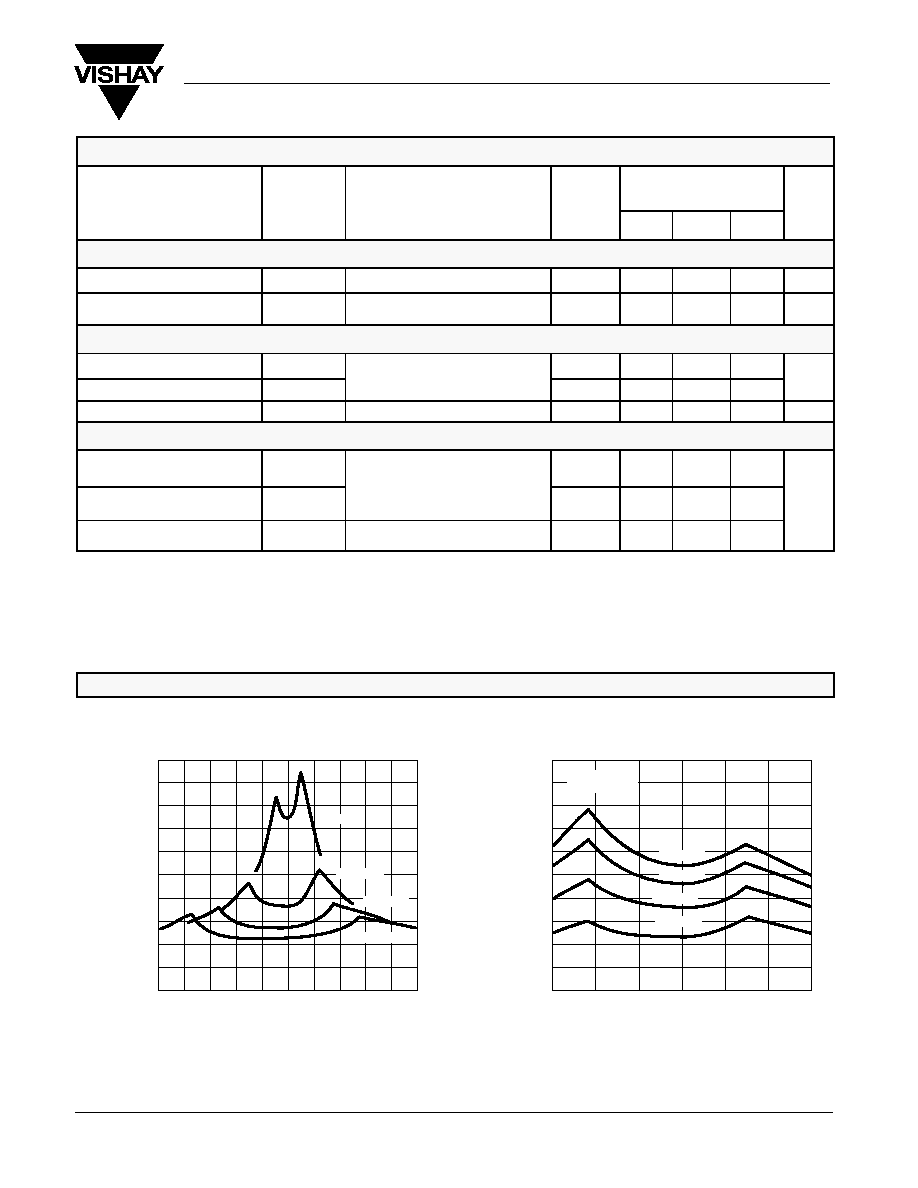
TYPICAL CHARACTERISTICS (25_C UNLESS NOTED)
85_C
-20 -16 -12 -8
-4
0
4
8
12
16
20
40
50
60
70
80
90
100
110
0
10
20
30
40
50
-15
-10
-5
0
5
10
15
"5 V
r
DS(on)
vs. V
D
and Power Supply Voltages
V
D
- Drain Voltage (V)
"10 V
"15 V
"20 V
r
DS(on)
vs. V
D
and Temperature
V
D
- Drain Voltage (V)
125_C
25_C
-55_C
V+ = 15 V
V- = -15 V
30
20
10
60
70
80
90
100
r DS(on)
-
Drain-Source On-Resistance (
)
W
r DS(on)
-
Drain-Source On-Resistance (
)
W

DG444B/445B
Vishay Siliconix
New Product
www.vishay.com
4
Document Number: 72626
S-32554--Rev. A, 15-Dec-03
TYPICAL CHARACTERISTICS (25_C UNLESS NOTED)
0
2
4
6
8
10
12
14
16
0
25
50
75
100
125
150
175
200
225
r
DS(on)
vs. V
D
and Single Power Supply Voltages
V
D
- Drain Voltage (V)
V+ = 5 V
7 V
10 V
12 V
15 V
250
-20
-15
-10
-5
0
5
10
15
20
40
20
0
-20
-40
Leakage Currents vs. Analog Voltage
I S,
I D
-
Current (pA)
I
S(off)
, I
D(off)
I
D(on)
-55
25
45
5
-15
65
1 nA
100 pA
10 pA
-35
1 pA
85
105 125
V+ = 15 V
V- = -15 V
V
S,
V
D
= "14 V
I
S(off)
, I
D(off)
I S,
I D
-
Current
Temperature (_C)
Leakage Current vs. Temperature
r DS(on)
-
Drain-Source On-Resistance (
)
W
V
ANALOG
- Analog Voltage (V)
V+ = 22 V
V- = -22 V
T
A
= 25_C
30
10
-10
-30
-15
-10
-5
0
5
10
15
30
20
10
0
-10
-20
-30
V+ = 15 V
V- = -15 V
V+ = 12 V
V- = 0 V
Q
-
Charge (pC)
Q
S,
Q
D
- Charge Injection vs. Analog Voltage
V
ANALOG
- Analog Voltage (V)
OIRR (dB)
10 k
100 k
1 M
10 M
40
50
60
70
80
90
100
110
120
f - Frequency (Hz)
Off Isolation vs. Frequency
V+ = +15 V
V- = -15 V
R
L
= 50 W
DG444B/445B
Vishay Siliconix
New Product
Document Number: 72626
S-32554--Rev. A, 15-Dec-03
www.vishay.com
5
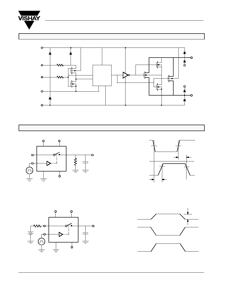
SCHEMATIC DIAGRAM (TYPICAL CHANNEL)
FIGURE 1.
Level
Shift/
Drive
V
IN
V
L
S
V+
GND
V-
D
V-
V+
TEST CIRCUITS
FIGURE 2. Switching Time
FIGURE 3. Charge Injection
0 V
Logic
Input
Switch
Input
Switch
Output
3 V
50%
0 V
V
O
V
S
t
r
<20 ns
t
f
<20 ns
t
OFF
t
ON
Note:
Logic input waveform is inverted for DG445.
OFF
ON
OFF
OFF
ON
OFF
V
O
DV
O
IN
X
IN
X
Q = DV
O
x C
L
(DG444B)
(DG445B)
50%
80%
80%
"10 V
C
L
(includes fixture and stray capacitance)
V-
V
L
IN
S
D
3 V
R
L
1 kW
C
L
35 pF
V
O
-15 V
GND
+5 V
C
L
1 nF
IN
D
V
O
V-
V+
S
3 V
V
g
R
g
-15 V
GND
+15 V
V+
+15 V
V
L
+5 V