 | –≠–ª–µ–∫—Ç—Ä–æ–Ω–Ω—ã–π –∫–æ–º–ø–æ–Ω–µ–Ω—Ç: DG485DN | –°–∫–∞—á–∞—Ç—å:  PDF PDF  ZIP ZIP |
DG485
Vishay Siliconix
Document Number: 70065
S-52433--Rev. E, 06-Sep-99
www.vishay.com
S
FaxBack 408-970-5600
5-1
Octal Analog Switch Array
FEATURES
BENEFITS
APPLICATIONS
D
Low On-Resistance: 55
W
D
Rail-to-Rail Analog Input Range
D
Serial Interface
D
Low-Power--P
D
: 35 nW
D
TTL and CMOS Compatible
D
Any Combination of 8 SPST to the
Output
D
High Speed--t
ON
: 170 ns
D
Low Signal Distortion
D
Devices Can Be Chained for System
Expansion
D
Reduced Board Space
D
Reduced Switch Errors
D
Reduced Power Supply
Requirements
D
Simple Interfacing
D
Audio Switching and Routing
D
Audio Teleconferencing
D
Data Acquisition and Industrial
Process Control
D
Battery Powered Remote Systems
D
Automotive, Avionics and ATE
Systems
D
Summing Amplifiers
DESCRIPTION
The DG485 is an analog switch array consisting of eight SPST
switches connected to a common output. This device may be
used as an 8-channel multiplexer in serial control applications.
Any, all or none of the eight switches may be closed at any
given time. Combining low on-resistance (r
DS(on)
55
W
, typ.)
and fast switching (t
ON
: 170 ns, typ.), the DG485 is ideally
suited for data acquisition, process control, communication,
and avionic applications.
Control data is input serially into the shift register with each
clock pulse. The shift register contents can be latched-in (via
LD) at any point into an octal latch which in turn controls all
switches. RS resets the shift register, forcing all latch inputs to
a low condition (all switches off). The serial input (D
IN
) and
serial output (D
OUT
) allow daisy chaining of multiple arrays for
large systems.
Built on the Vishay Siliconix high voltage silicon gate process
the DG485 has a wide 44-V power supply voltage rating. An
epitaxial layer prevents latchup.
Each channel conducts equally well in either direction when on
and blocks up to rail-to-rail voltages when off.
For additional information please refer to application note
AN204.
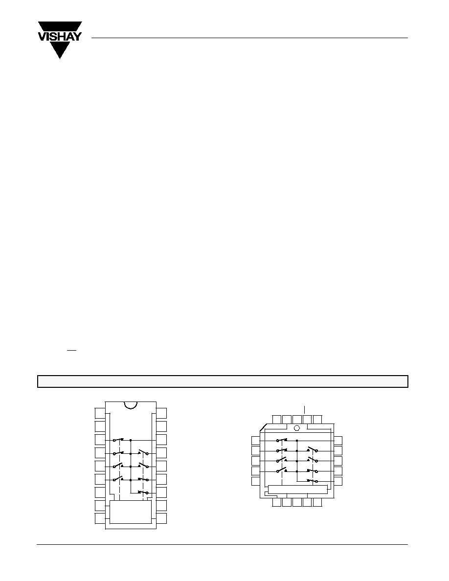
FUNCTIONAL BLOCK DIAGRAM AND PIN CONFIGURATION
1
2
3
4
5
6
7
8
18
17
16
15
14
13
12
11
LD
RS
V
L
GND
S
4
D
S
3
S
5
S
2
S
6
S
1
S
7
V+
S
8
D
IN
V≠
Dual-In-Line
Top View
9
10
CLK
D
OUT
Shift Register
Latches
PLCC and LCC
14
15
16
17
18
8
7
6
5
4
1
2
3
19
20
11
10
9
13
12
Top View
S
4
D
S
3
S
5
S
2
S
6
S
1
S
7
V+
S
8
IN
CLK
NC
OUT
V
LD
NC
RS
GND
Shift Register/Latches
L
D
D
V≠

DG485
Vishay Siliconix
www.vishay.com
S
FaxBack 408-970-5600
5-2
Document Number: 70065
S-52433--Rev. E, 06-Sep-99
TRUTH TABLES AND ORDERING INFORMATION
TRUTH TABLE DUAL IN LINE PACKAGE
RS
CLK*
D
IN
D
1
D
n
1
0
0
D
n-1
1
1
1
D
n-1
1
X
D
1
D
n
(No Change)
0
X
X
0
0
*CLK Input Edge Triggered
TRUTH TABLE PLCC & LCC PACKAGES
LD*
D
n
L
n
SW
n
0
0
OFF
1
1
ON
D
n
L
n
(No Change)
*LD Input Level Triggered
ORDERING INFORMATION
Temp Range
Package
Part Number
≠40 to 85
_
C
18-Pin Plastic DIP
DG485DJ
≠40 to 85
_
C
20-Pin PLCC
DG485DN
≠55 to 125
_
C
LCC-20
DG485AZ/883
ABSOLUTE MAXIMUM RATINGS
Voltages Referenced to V≠
V+
44 V
. . . . . . . . . . . . . . . . . . . . . . . . . . . . . . . . . . . . . . . . . . . . . . . . . . . . . . . . . . .
GND
25 V
. . . . . . . . . . . . . . . . . . . . . . . . . . . . . . . . . . . . . . . . . . . . . . . . . . . . . . . . .
Digital Inputs
a
V
S
, V
D
(V≠) ≠2 V to (V+) + 2 V
. . . . . . . . . . . . . . . . . . . . . . . . . .
or 30 mA, whichever occurs first
Continuous Current (Any Terminal)
30 mA
. . . . . . . . . . . . . . . . . . . . . . . . . . . . .
Current, S or D (Pulsed 1 ms, 10% duty cycle)
100 mA
. . . . . . . . . . . . . . . . . .
Storage Temperature
(AZ Suffix)
≠65 to 150
_
C
. . . . . . . . . . . . . . . . . .
(DJ, DN Suffix)
≠65 to 125
_
C
. . . . . . . . . . . . . .
Power Dissipation (Package)
b
18-Pin Plastic DIP
c
470 mW
. . . . . . . . . . . . . . . . . . . . . . . . . . . . . . . . . . . . . . . . .
20-Pin PLCC, LCC
d
800 mW
. . . . . . . . . . . . . . . . . . . . . . . . . . . . . . . . . . . . . . . .
Notes:
a.
Signals on S
X
, D
X
or IN
X
exceeding V+ or V≠ will be clamped by internal
diodes. Limit forward diode current to maximum current ratings.
b.
All leads soldered or welded to PC board.
c.
Derate 6 mW/
_
C above 75
_
C.
d.
Derate 10 mW/
_
C above 75
_
C.
DG485
Vishay Siliconix
Document Number: 70065
S-52433--Rev. E, 06-Sep-99
www.vishay.com
S
FaxBack 408-970-5600
5-3
SPECIFICATIONS
a
Test Conditions
Unless Otherwise Specified
A Suffix
≠55 to 125
_
C
D Suffix
≠40 to 85
_
C
Parameter
Symbol
V+ = 15 V, V≠ = ≠15 V
V
L
= 5 V, V
IN
= 2.4 V, 0.8 V
f
Temp
b
Typ
c
Min
d
Max
d
Min
d
Max
d
Unit
Analog Switch
Analog Signal Range
e
V
ANALOG
Full
≠15
15
≠15
15
V
Drain-Source
On-Resistance
r
DS(on)
V+ = 13.5 V, V≠ = ≠13.5 V
I
S
= ≠5 mA, V
D
=
"
10 V
Room
Full
55
85
125
85
125
W
Delta Drain-Source
On-Resistance
g
D
r
DS(on)
Room
6
%
Switch Off
L
k
C
t
I
S(off)
V+ = 16.5 V, V≠ = ≠16.5 V
V
15 5 V V
15 5 V
Room
Full
0.01
≠1
≠20
1
20
≠1
≠10
1
10
A
Leakage Current
I
D(off)
,
V
D
=
#
15.5 V, V
S
=
"
15.5 V
Room
Full
0.1
≠10
≠200
10
200
≠10
≠50
10
50
nA
Channel On
L
k
C
t
I
D(on)
V
"
=
"
16.5 V V
S
= V
D
=
"
15.5 V
One Switch At A Time
Room
Full
0.11
≠20
≠500
20
500
≠20
≠50
20
50
nA
Leakage Current
I
D(on)
V
"
=
"
16.5 V, V
S
= V
D
=
"
15.5 V
All Switches On
Room
0.2
Input
Input Current
with V
IN
Low
I
IL
V
IN
Under Test = 0.8 V
All Other = 2.4 V
Room
Full
≠0.0001
≠1
≠5
1
5
≠1
≠5
1
5
m
A
Input Current
with V
IN
High
I
IH
V
IN
Under Test = 2.4 V
All Other = 0.8 V
Room
Full
0.0001
≠1
≠5
1
5
≠1
≠5
1
5
Serial Data Output
Output Voltage
with V
IN
Low ≠ D
OUT
V
OL
I
O
= 1.6 mA, V+ = 4.5 V
Full
0.25
0.4
0.4
V
Output Voltage
with V
IN
High ≠ D
OUT
V
OH
I
O
= ≠80
m
A, V+ = 16.5 V
V
L
= 4.75 V
Full
4.4
2.7
2.7
V
Dynamic Characteristics
Turn-On Time
t
ON
V
S
=
"
10 V
See Figures 1, 8
Room
Full
170
200
275
200
275
Turn-Off Time
t
OFF
V
S
=
"
10 V
See Figures 2, 3, 8
Room
Full
150
200
275
200
276
Data Setup Time
t
DS
See Figures 4, 8
Room
Full
40
60
40
60
Data Hold Time
t
DH
See Figures 4, 8
Room
Full
40
60
40
60
ns
LOAD Hold Time
t
LH
S
Fi
5 8
Room
Full
100
150
100
150
RESET Hold Time
t
RH
See Figures 5, 8
Room
Full
100
150
100
150
RESET
"
to CLOCK
"
Delay
t
DRC
Room
Full
40
60
40
60
Charge Injection
Q
V
S
= 0 V, C
L
= 1,000 pF
Any One Channel
Room
17
pC
Off Isolation
e
OIRR
R
L
= 50
W
, C
L
= 5 pF, f = 1 MHz
See Figure 9
Room
≠75
dB
Maximum
Clock Frequency
f
CLK
Room
10
MHz
DG485
Vishay Siliconix
www.vishay.com
S
FaxBack 408-970-5600
5-4
Document Number: 70065
S-52433--Rev. E, 06-Sep-99
SPECIFICATIONS
a
Test Conditions
Unless Otherwise Specified
A Suffix
≠55 to 125
_
C
D Suffix
≠40 to 85
_
C
Parameter
Symbol
V+ = 15 V, V≠ = ≠15 V
V
L
= 5 V, V
IN
= 2.4 V, 0.8 V
f
Temp
b
Typ
c
Min
d
Max
d
Min
d
Max
d
Unit
Dynamic Characteristics (Cont'd)
Source Off
Capacitance
e
C
S(off)
V
gen
= 0 V, R
gen
= 0
W,
f = 1 MHz
Room
7
F
Drain Off Capacitance
e
C
D(off)
gen
,
gen
Room
43
F
On-State Capacitance
e
C
D(on)
V
gen
= 0 V, R
gen
= 0
W
, f = 1 MHz One
Channel On
Room
53
pF
On-State Capacitance
e
C
D(on)
V
gen
= 0 V, R
gen
= 0
W
, f = 1 MHz All Chan-
nels On
Room
122
Power Supplies
Positive Supply
Current
I+
V
16 5 V V
16 5 V
Room
Full
0.001
3
10
3
10
A
Negative Supply
Current
I≠
V+ = 16.5 V, V≠ = ≠16.5 V
V
IN
= 0 or 5 V, V
L
= 5.25 V
Room
Full
≠0.001
≠3
≠10
≠3
≠10
m
A
Logic Supply Current
I
L
V
IN
= 0 or 5 V, V
L
= 5.25 V
D
OUT
Open
Room
Full
0.001
3
10
3
10
m
A
Ground Current
I
GND
Room
Full
≠0.001
≠3
≠10
≠3
≠10
Notes:
a.
Refer to PROCESS OPTION FLOWCHART.
b.
Room = 25
_
C, Full = as determined by the operating temperature suffix.
c.
Typical values are for DESIGN AID ONLY, not guaranteed nor subject to production testing.
d.
The algebraic convention whereby the most negative value is a minimum and the most positive a maximum, is used in this data sheet.
e.
Guaranteed by design, not subject to production test.
f.
V
IN
= input voltage to perform proper function.
g.
For each V
D
:
D
r
DS(on)
+
r
DS(on)
MAX ≠ r
DS(on)
MIN
r
DS(on)
AVE
TYPICAL CHARACTERISTICS (25_C UNLESS NOTED)
GND
Supply Currents vs. Temperature
r
DS(on)
vs. V
D
and Power Supply Voltage
I+, I≠, I
r DS(on)
≠ Drain-Source On-Resistance (
Temperature (
_
C)
V
D
≠ Drain Voltage (V)
V+ = 15 V
V≠ = ≠15 V
V
L
= 5 V
I
L
I
POS
I
GND
≠50
≠10
130
160
140
0
≠20
≠10
0
10
20
120
100
80
60
40
20
≠30
10
30
50
70
90
110
1 mA
100 nA
V
L
= 5 V
I
S
= ≠5 mA
"
5 V
10 nA
1 nA
100 pA
10 pA
1 pA
0.1 pA
I
NEG
"
8 V
"
10 V
"
12 V
"
15 V
"
20 V
≠15
≠5
5
15
)
W
DG485
Vishay Siliconix
Document Number: 70065
S-52433--Rev. E, 06-Sep-99
www.vishay.com
S
FaxBack 408-970-5600
5-5
TYPICAL CHARACTERISTICS (25_C UNLESS NOTED)
r
DS(on)
vs. V
D
and Unipolar Power Supply Voltage
r
DS(on)
vs. V
D
and Temperature
Switching Threshold
vs. Power Supply Voltage and V
L
RF Characteristics
Channel On/Off Leakage Currents
vs. Analog Voltage
Channel On/Off Leakage Currents
vs. Temperature
r DS(on)
≠ Drain-Source On-Resistance (
r DS(on)
≠ Drain-Source On-Resistance (
I
, I
SD
(pA)
, I
S + D
I
, I
DS
(dB)
(V)
TH
V
V
D
≠ Drain Voltage (V)
V
D
≠ Drain Voltage (V)
V
D
or V
S
≠ Drain or Source Voltage (V)
Temperature (
_
C)
V+ Supply (V)
f ≠ Frequency (Hz)
100
90
70
20
0
≠15
≠10
≠5
0
5
10
15
80
60
10
30
50
40
400
350
0
0
2
20
300
250
200
150
100
50
4
6
8
10
12
14
16
18
V+ = 5 V
8 V
10 V
12 V
15 V
20 V
V≠ = 0 V
V
L
= 5 V
I
S
= ≠5 mA
V+ = 15 V
V≠ = ≠15 V
V
L
= 5 V
I
S
= ≠5 mA
125
_
C
25
_
C
≠55
_
C
60
40
20
≠80
≠15
≠10
15
0
≠20
≠5
0
5
10
≠40
≠60
V+ = 15 V
V≠ = ≠15 V
V
L
= 5 V
I
S(off)
I
D(off)
I
D(on)
1 mA
100 nA
1 nA
100 pA
10 pA
1 pA
0.1 pA
0.01 pA
≠50
≠10
130
≠30
10
30
50
70
90
110
V+ = 15 V
V≠ = ≠15 V
V
L
= 5 V
V
S
or V
D
= ≠ 14 V
I
D(off)
I
S(off)
I
D(on)
10 nA
3.0
2.5
2.0
0.5
0
5
6
1.0
1.5
7
8
9
10
11
12
13
14
15
4 V
5 V
6 V
6 V
V
L
= 7 V
≠140
≠120
0
≠100
≠80
≠60
≠40
≠20
OIRR
X
TALK
V+ = 15 V
V≠ = ≠15 V
V
L
= 5 V
See Figures 9, 10
1 k
10 k
100 k
1 M
10 M
)
W
)
W