 | –≠–ª–µ–∫—Ç—Ä–æ–Ω–Ω—ã–π –∫–æ–º–ø–æ–Ω–µ–Ω—Ç: DG9051 | –°–∫–∞—á–∞—Ç—å:  PDF PDF  ZIP ZIP |
Vishay Siliconix
DG9051/9052/9053
New Product
Document Number: 73410
S-52072-Rev. A, 10-Oct-05
www.vishay.com
1
Precision 8-Ch/Dual 4-Ch/Triple 2-Ch
Low Voltage Analog Switches/Multiplexers
FEATURES
∑
2.7 to 12-V Single Supply
or ±2.7 to ±6-V Dual Supply Operation
∑
Guaranteed Ron Matching
∑
Low Voltage CMOS Logic Compatible
BENEFITS
∑
Wide Operation Voltage Range
∑
Pin Compatible with 74HC4051/2/5
∑
Guaranteed Low Leakage
APPLICATIONS
∑
Battery Powered Equipment
∑
Test Process Equipment
∑
Communication Systems
∑
A/V and Mixed Signal Routing
∑
Automotive
DESCRIPTION
The DG9051/9052/9053 are low-voltage monolithic CMOS
analog switches and multiplexers. DG9051 is an 8-channel
multiplexer; DG9052 is a dual 4-channel multiplexer; and
DG9053 is a triple single-pole/double throw (SPDT) switch.
They are designed to operate from a +2.7 to +12-V single
supply or ±2.7 to ±6-V dual power supplies. All control logic
inputs have guaranteed 2-V logic high/0.8-V logic low when
operating from a single 5 V or dual ±5-V supplies, and 2.4-V
logic high/0.8-V logic low when V + = 12 V.
Built on Vishay Siliconix's proprietary high-density process,
the DG9051/9052/9053 offer the advantage of bi-directional
signal, rail to rail analog signal handling.
As a committed partner to the community and the environ-
ment, Vishay Siliconix manufactures this product with the
Lead (Pb)-Free device terminations. For analog switching
products manufactured with 100 % matte tin device termina-
tion, the Lead (Pb)-Free "-E3"suffix is being used as a de-
signator.
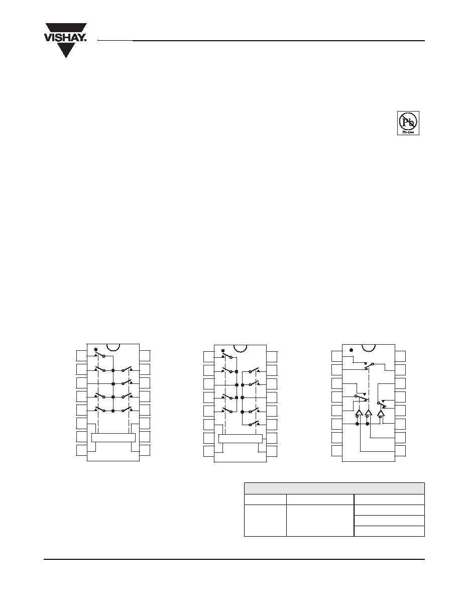
FUNCTIONAL BLOCK DIAGRAM AND PIN CONFIGURATION
The information shown here is a preliminary product proposal, not a commercial product data sheet. Siliconix is not committed to produce this or
any similiar product. This information should not be used for design purposes, nor construed as an offer to furnish or sell such products
Enable
Y1
A
GND
V
EE
V
CC
C
B
Y0
Y
Z1
X
Z
X1
Z0
X0
1
2
3
4
5
6
8
9
7
16
15
14
13
12
11
10
DG9053
Enable
Y0
X3
GND
V
EE
V
CC
B
A
Y2
X2
Y
X1
Y3
X
Y1
X0
1
2
3
4
5
6
8
9
7
16
15
14
13
12
11
10
DG9052
Logic
Enable
X4
A
GND
V
EE
V
CC
C
B
X6
X2
X
X1
X7
X0
X5
X3
1
2
3
4
5
6
8
7
16
15
14
13
12
11
9
10
DG9051
Logic
ORDERING INFORMATION
Temp Range
Package
Part Number
≠40 to 85∞C
TSSOP≠16
DG9051DQ≠T1≠E3
DG9052DQ≠T1≠E3
DG9053DQ≠T1≠E3
RoHS
COMPLIANT
www.vishay.com
2
Document Number: 73410
S-52072-Rev. A, 10-Oct-05
Vishay Siliconix
DG9051/9052/9053
New Product
X = Don't care
TRUTH TABLE
Enable
Input
Select Inputs
On Switches
C*
B
A
DG9051
DG9052
DG9053
H
X
X
X
All switches open
All switches open
All switches open
L
L
L
L
X ≠ X0
X ≠ X0,
Y ≠ Y0
X ≠ X0,
Y ≠ Y0,
Z ≠ Z0
L
L
L
H
X ≠ X1
X ≠ X1,
Y ≠ Y1
X ≠ X1,
Y ≠ Y0,
Z ≠ Z0
L
L
H
L
X ≠ X2
X ≠ X2,
Y ≠ Y2
X ≠ X0,
Y ≠ Y1,
Z ≠ Z0
L
L
H
H
X ≠ X3
X ≠ X3,
Y ≠ Y3
X ≠ X1,
Y ≠ Y1,
Z ≠ Z0
L
H
L
L
X ≠ X4
X ≠ X0,
Y ≠ Y0
X ≠ X0,
Y ≠ Y0,
Z≠ Z1
L
H
L
H
X ≠ X5
X ≠ X1,
Y ≠ Y1
X ≠ X1,
Y ≠ Y0,
Z ≠ Z1
L
H
H
L
X ≠ X6
X ≠ X2,
Y ≠ Y2
X ≠ X0,
Y ≠ Y1,
Z ≠ Z1
L
H
H
H
X ≠ X7
X ≠ X3,
Y ≠ Y3
X ≠ X1,
Y ≠ Y1,
Z ≠ Z1
ABSOLUTE MAXIMUM RATINGS T
A
= 25 ∞C, unless otherwise noted
Parameter Symbol
Limit
Unit
Voltage Referenced to V≠
V+
13.5
V
GND
7
Digital Inputs
a
V
S
, V
D
(V≠) ≠0.3 to (V+) +0.3
Current (Any Terminal Except S or D)
30
mA
Continuous Current, S or D
100
Peak Current, S or D (Pulsed at 1 ms, 10 % Duty Cycle Max)
200
Package Solder Reflow Conditions
b
IR/Convection
260
∞C
Storage Temperature
≠65 to 150
Power Dissipation (Packages)
c
T
A
= 70 ∞C, TSSOP-16
d
925
mW

Document Number: 73410
S-52072-Rev. A, 10-Oct-05
www.vishay.com
3
Vishay Siliconix
DG9051/9052/9053
New Product
SPECIFICATIONS (SINGLE SUPPLY 12 V)
Parameter Symbol
Test Condition
Otherwise Unless Specified
V+ = 12 V, ±10 %, V≠ = 0 V
V
A
, V
EN
= 0.8 V or 2.4 V
f
Temp
b
Limits
≠40 to 85∞C
Unit
Min
c
Typ
d
Max
c
Analog Switch
Analog Signal Range
e
V
ANALOG
Full
0
12
V
On-Resistance
r
ON
V
D
= 3.5 V, I
S
= 1 mA
Sequence Each Switch On
Room
Full
30
40
50
r
ON
Match Between Channels
g
r
ON
V
D
= 3.5 V, I
S
= 1 mA
Room
5
Switch Off Leakage Current
I
S(off)
V
EN
= 2.4 V, V
D
= 11 V or 1 V, V
S
= 1 V or 11 V
Room
Full
≠1
≠20
1
20
nA
I
D(off)
Room
Full
≠1
≠20
1
20
Channel On Leakage Current
I
D(on)
V
EN
= 0 V, V
S
= V
D
= 1 V or 11 V
Room
Full
≠2
≠10
2
10
Digital Control
Logic High Input Voltage
V
INH
Full
2.4
V
Logic Low Input Voltage
V
INL
Full
0.8
Input Current
I
IN
V
AX
= V
EN
= 2.4 V or 0.8 V
Full
≠1
1
µA
Dynamic Characteristics
Transition Time
t
TRANS
V
NO
/V
NC
= 8 V/0 V, 0 V/8 V
R
L
= 300
, C
L
= 35 pF
Room
Full
26
35
55
ns
Break-Before-Make Time
t
BBM
V
X,Y, Z
= 5 V, V
S
= 0 V,
R
L
= 306
, C
L
= 35 pF
Room
Full
3
10
Enable Turn-On Time
t
ON(EN)
Room
Full
20
35
45
Enable Turn-Off Time
t
OFF(EN)
Room
Full
16
30
40
Charge Injection
e
Q
C
L
= 1 nF, V
GEN
= 0 V, R
GEN
= 0
Room
38
pC
Off-Isolation
e,h
OIRR
f = 1 MHz, R
L
= 50
Room
≠78
dB
Crosstalk
e
X
TALK
Room
≠83
Source Off Capacitance
e
C
S(off)
f = 1 MHz, V
S
= 0 V, V
EN
= 2.4 V
Room
4
pF
Drain Off Capacitance
e
C
D(off)
f = 1 MHz, V
D
= 0 V, V
EN
= 2.4 V
Room
8
Drain On Capacitance
e
C
D(on)
f = 1 MHz, V
D
= 0 V, V
EN
= 0 V
Room
15
Power Supply
Power Supply Current
I+
V
EN
= V
A
= 0 V or V+
Room
1.0
µA

www.vishay.com
4
Document Number: 73410
S-52072-Rev. A, 10-Oct-05
Vishay Siliconix
DG9051/9052/9053
New Product
SPECIFICATIONS (DUAL SUPPLY V+ = 5 V, V
≠
=
≠
5 V)
Parameter Symbol
Test Condition
Otherwise Unless Specified
V+ = 5 V, V≠ = ≠5 V ±10 %
V
A
, V
EN
= 0.8 V or 2.0 V
f
Temp
b
Limits
≠40 to 85∞C
Unit
Min
c
Typ
d
Max
c
Analog Switch
Analog Signal Range
e
V
ANALOG
Full
≠5
5
V
On-Resistance
r
ON
V+ = 4.5 V, V≠ = ≠4.5 V, V
D
= ±3 V, I
S
= 1 mA
Sequence Each Switch On
Room
Full
35
55
60
r
ON
Match Between Channels
g
r
ON
V+ = 4.5 V, V≠ = ≠4.5 V, V
D
= ±3.0 V, I
S
= 1 mA
Room
5
On-Resistance Flatness
i
r
ON
Flatness
Room
7
10
Switch Off Leakage Current
a
I
S(off)
V+ = 5.5 V, V≠ = ≠5.5 V
V
EN
= 2.0 V, V
D
= ±4.5 V, V
S
= ±4.5 V
Room
Full
≠1
≠20
1
20
nA
I
D(off)
Room
Full
≠1
≠20
1
20
Channel On Leakage Current
a
I
D(on)
V+ = 5.5 V, V≠ = ≠5.5 V
V
EN
= 0 V, V
D
= ±4.5 V, V
S
= ±4.5 V
Room
Full
≠2
≠10
2
10
Digital Control
Logic High Input Voltage
V
INH
Full
2.0
V
Logic Low Input Voltage
V
INL
Full
0.8
Input Current
a
I
IN
V
AX
= V
EN
= 2.0 V or 0.8 V
Full
≠1
1
µA
Dynamic Characteristics
Transition Time
e
t
TRANS
V+ = 4.5 V, V≠ = ≠4.5 V V
NO/NC
= ±3 V,
R
L
= 300
, C
L
= 35 pF
Room
Full
35
50
65
ns
Break-Before-Make Time
e
t
BBM
V
X,Y, Z
= +/≠3 V, V
S
= 0 V,
R
L
= 300
, C
L
= 35 pF
Room
Full
5
12
Enable Turn-On Time
e
t
ON(EN)
Room
Full
38
55
70
Enable Turn-Off Time
e
t
OFF(EN)
Room
Full
22
35
50
Source Off Capacitance
e
C
S(off)
f = 1 MHz, V
S
= 0 V, V
EN
= 2.0 V
Room
5
pF
Drain Off Capacitance
e
C
D(off)
f = 1 MHz, V
D
= 0 V, V
EN
= 2.0 V
Room
9
Drain On Capacitance
e
C
D(on)
f = 1 MHz, V
D
= 0 V, V
EN
= 0 V
Room
13
Power Supply
Power Supply Current
I+
V
EN
= V
A
= 0 V or V+
Room
1.0
µA
I≠
Room
≠1.0

Document Number: 73410
S-52072-Rev. A, 10-Oct-05
www.vishay.com
5
Vishay Siliconix
DG9051/9052/9053
New Product
SPECIFICATIONS (SINGLE SUPPLY 5 V)
Parameter Symbol
Test Condition
Otherwise Unless Specified
V+ = 5 V, ±10 %, V≠ = 0 V
V
A
, V
EN
= 0.8 V or 2.0 V
f
Temp
b
Limits
≠40 to 85∞C
Unit
Min
c
Typ
d
Max
c
Analog Switch
Analog Signal Range
e
V
ANALOG
Full
0
5
V
On-Resistance
r
ON
V+ = 4.5 V, V
D
or V
S
= 3 V or 3.5 V, I
S
= 1 mA
Room
Full
80
100
120
r
ON
Match Between Channels
g
r
ON
V+ = 4.5 V, V
D
= 3 V, I
S
= 1 mA
Room
8.0
Switch Off Leakage Current
a
I
S(off)
V+ = 5.5 V, V
EN
= 2 V
V
S
= 1 V or 4.5 V, V
D
= 4.5 V or 1 V
Room
Full
≠1
≠20
1
20
nA
I
D(off)
Room
Full
≠1
≠20
1
20
Channel On Leakage Current
a
I
D(on)
V+ = 5.5 V, V
EN
= 0 V
V
D
= V
S
= 1 V or 4.5 V
Room
Full
≠2
≠10
2
10
Digital Control
Logic High Input Voltage
V
INH
Full
2.0
V
Logic Low Input Voltage
V
INL
Full
0.8
Input Current
a
I
IN
V
AX
= V
EN
= 2.0 V or 0.8 V
Full
≠1
1
µA
Dynamic Characteristics
Transition Time
t
TRANS
V+ = 4.5 V, V≠ = 0 V, V
NO / NC
= 3 V / 0 V,
0 V / 3 V, R
L
= 300
, C
L
= 35 pF
Room
40
ns
Break-Before-Make Time
t
BBM
V+ = 4.5 V, V
X,Y, Z
= 3 V, V
S
= 0 V,
R
L
= 300
, C
L
= 35 pF
Room
15
Enable Turn-On Time
t
ON(EN)
Room
40
Enable Turn-Off Time
t
OFF(EN)
Room
20
Charge Injection
e
Q
C
L
= 1 nF, V
GEN
= 0 V, R
GEN
= 0
Room
20
pC
Off-Isolation
e,h
OIRR
f = 1 MHz, R
L
= 50
Room
≠79
dB
Crosstalk
e
X
TALK
Room
≠83
Source Off Capacitance
e
C
S(off)
f = 1 MHz, V
S
= 0 V, V
EN
= 0 V
Room
4
pF
Drain Off Capacitance
e
C
D(off)
f = 1 MHz, V
D
= 0 V, V
EN
= 2.0 V
Room
8
Drain On Capacitance
e
C
D(on)
f = 1 MHz, V
D
= 0 V, V
EN
= 0 V
Room
15
Power Supply
Power Supply Current
I+
V
EN
= V
A
= 0 V or V+
Room
1.0
µA