DG9232/9233
Vishay Siliconix
Document Number: 70837
S-05298--Rev. D, 17-Dec-01
www.vishay.com
1
Low-Voltage Dual SPST Analog Switch
FEATURES
D
Low Voltage Operation (+2.7 to +5 V)
D
Low On-Resistance - r
DS(on
): 20
W
D
Fast Switching - t
ON
: 35 ns, t
OFF
: 20 ns
D
Low Leakage - I
COM(on)
: 200-pA max
D
Low Charge Injection - Q
INJ
: 1 pC
D
Low Power Consumption
D
TTL/CMOS Compatible
D
ESD Protection > 2000 V (Method 3015.7)
D
Available in MSOP-8 and SOIC-8
BENEFITS
D
Reduced Power Consumption
D
Simple Logic Interface
D
High Accuracy
D
Reduce Board Space
APPLICATIONS
D
Battery Operated Systems
D
Portable Test Equipment
D
Sample and Hold Circuits
D
Cellular Phones
D
Communication Systems
D
Military Radio
D
PBX, PABX Guidance and
Control Systems
DESCRIPTION
The DG9232/9233 is a single-pole/single-throw monolithic
CMOS analog device designed for high performance
switching of analog signals. Combining low power, high speed
(t
ON
: 35 ns, t
OFF
: 20 ns), low on-resistance (r
DS(on)
: 20
W
)
and small physical size, the DG9232/9233 is ideal for portable
and battery powered applications requiring high performance
and efficient use of board space.
The DG9232/9233 is built on Vishay Siliconix's low voltage
BCD-15 process. Minimum ESD protection, per Method 3015.7 is
2000 V. An epitaxial layer prevents latchup. Break-before -make is
guaranteed for DG9232/9233.
Each switch conducts equally well in both directions when on,
and blocks up to the power supply level when off.
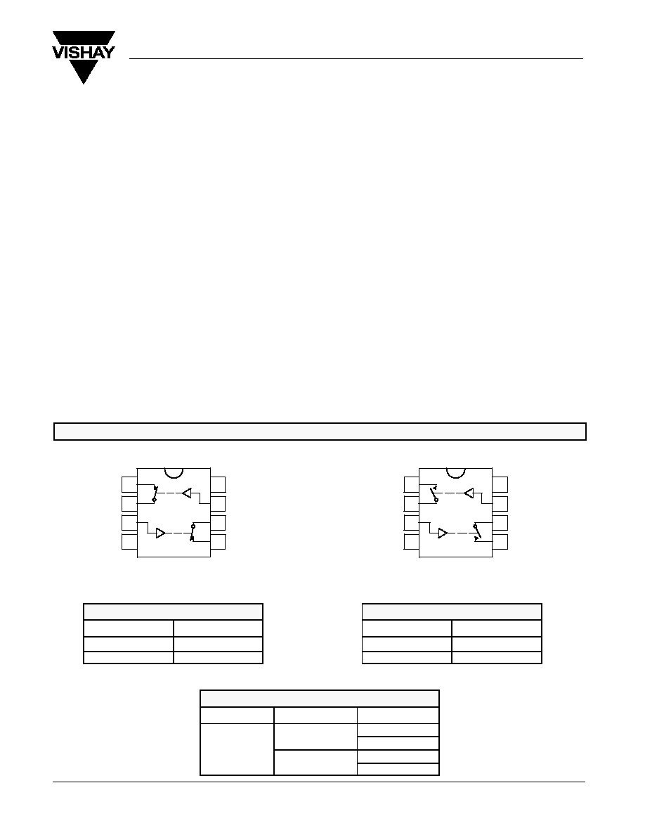
FUNCTIONAL BLOCK DIAGRAM AND PIN CONFIGURATION
NO
1
V+
COM
1
IN
1
IN
2
COM
2
GND
NO
2
1
2
3
4
8
7
6
5
Top View
NC
1
V+
COM
1
IN
1
IN
2
COM
2
GND
NC
2
1
2
3
4
8
7
6
5
Top View
TRUTH TABLE - DG9232
Logic
Switch
0
On
1
Off
Logic "0"
v
0.8 V
Logic "1"
w
2.4 V
TRUTH TABLE - DG9233
Logic
Switch
0
Off
1
On
Logic "0"
v
0.8 V
Logic "1"
w
2.4 V
ORDERING INFORMATION
Temp Range
Package
Part Number
DG9232DY
�
SOIC-8
DG9233DY
-40 to 85
�
C
DG9232DQ
MSOP-8
DG9233DQ
DG9232/9233
Vishay Siliconix
www.vishay.com
2
Document Number: 70837
S-05298--Rev. D, 17-Dec-01
ABSOLUTE MAXIMUM RATINGS
Reference to GND
V+
-0.3 to +13 V
. . . . . . . . . . . . . . . . . . . . . . . . . . . . . . . . . . . . . . . . . . . . . . . . . . .
IN, COM, NC, NO
a
-0.3 to (V+ + 0.3 V)
. . . . . . . . . . . . . . . . . . . . . . . . . . . . . . . . . . . . . . .
Continuous Current (Any terminal)
"
20 mA
. . . . . . . . . . . . . . . . . . . . . . . . . . .
Peak Current
"
40 mA
. . . . . . . . . . . . . . . . . . . . . . . . . . . . . . . . . . . . . . . . . . . . . .
(Pulsed at 1ms, 10% duty cycle)
ESD (Method 3015.7)
> 2000 V
. . . . . . . . . . . . . . . . . . . . . . . . . . . . . . . . . . . . . . .
Storage Temperature (D Suffix)
-65 to 125
�
C
. . . . . . . . . . . . . . . . . . . . . . . . . . . .
Power Dissipation (Packages)
b
8-Pin Narrow Body SOIC
c
400 mW
. . . . . . . . . . . . . . . . . . . . . . . . . . . . . . . . . . .
Notes:
a.
Signals on S
X
, D
X
, or IN
X
exceeding V+ or V- will be clamped by internal
diodes. Limit forward diode current to maximum current ratings.
b.
All leads welded or soldered to PC Board.
c.
Derate 6.5 mW/
_
C above 75
_
C
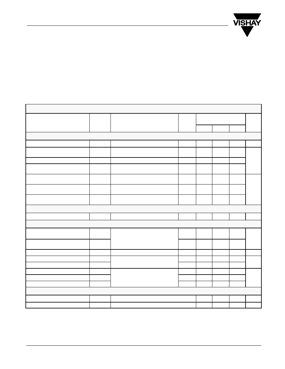
SPECIFICATIONS (V+ = 3 V)
Test Conditions
Otherwise Unless Specified
D Suffix
�40 to 85
_
C
Parameter
Symbol
V+ = 3 V,
"
10%, V
IN
= 0.8 or 2.4 V
e
Temp
a
Min
c
Typ
b
Max
c
Unit
Analog Switch
Analog Signal Range
d
V
ANALOG
Full
0
3
V
Drain-Source On-Resistance
r
DS(on)
V
NO
or V
NC
= 1.5 V, V+ = 2.7 V
I
COM
= 5 mA
Room
Full
30
50
80
r
DS(on)
Match
d
D
r
DS(on)
V
NO
or V
NC
= 1.5 V
Room
0.4
2
W
r
DS(on)
Flatness
d
r
DS(on)
Flatness
V
NO
or V
NC
= 1 and 2 V
Room
4
8
NO or NC Off Leakage Current
g
I
NO/NC(off)
V
NO
or V
NC
= 1 V / 2 V, V
COM
= 2 V / 1 V
Room
Full
-100
�5000
5
100
5000
COM Off Leakage Current
g
I
COM(off)
V
COM
= 1 V / 2 V, V
NO
or V
NC
= 2 V / 1 V
Room
Full
-100
�5000
5
100
5000
pA
Channel-On Leakage Current
g
I
COM(on)
V
COM
= V
NO
or V
NC
= 1 V / 2 V
Room
Full
-200
�10000
10
200
10000
Digital Control
Input Current
I
INL
or I
INH
Full
1
m
A
Dynamic Characteristics
Turn-On Time
t
ON
Room
Full
50
120
200
Turn-Off Time
t
OFF
V
NO
or V
NC
= 1.5 V
Room
Full
20
50
120
ns
Charge Injection
d
Q
INJ
C
L
= 1 nF, V
GEN
= 0 V, R
GEN
= 0
W
Room
1
5
pC
Off-Isolation
OIRR
W
Room
�74
Crosstalk
X
TALK
R
L
= 50
W
, C
L
= 5 pF, f = 1 MHz
Room
�90
dB
NC and NO Capacitance
C
(off)
Room
7
Channel-On Capacitance
C
COM(on)
f = 1 MHz
Room
20
pF
Com-Off Capacitance
C
COM(off)
Room
13
Power Supply
Power Supply Range
V+
2.7
12
V
Power Supply Current
I+
V+ = 3.3 V, V
IN
= 0 or 3.3 V
1
m
A
Notes:
a.
Room = 25
�
C, Full = as determined by the operating suffix.
b.
Typical values are for design aid only, not guaranteed nor subject to production testing.
c.
The algebraic convention whereby the most negative value is a minimum and the most positive a maximum, is used in this data sheet.
d.
Guarantee by design, nor subjected to production test.
e.
V
IN
= input voltage to perform proper function.
f.
Difference of min and max values.
g.
Guaranteed by 5-V leakage tests, not production tested.

DG9232/9233
Vishay Siliconix
Document Number: 70837
S-05298--Rev. D, 17-Dec-01
www.vishay.com
3
SPECIFICATIONS (V+ = 5 V)
Test Conditions
Otherwise Unless Specified
D Suffix
�40 to 85
_
C
Parameter
Symbol
V+ = 5 V,
"
10%, V
IN
= 0.8 or 2.4 V
e
Temp
a
Min
c
Typ
b
Max
c
Unit
Analog Switch
Analog Signal Range
d
V
ANALOG
Full
0
5
V
Drain-Source On-Resistance
r
DS(on)
V
NO
or V
NC
= 3.5 V, V+ = 4.5 V
I
COM
= 5 mA
Room
Full
20
30
50
r
DS(on)
Match
d
D
r
DS(on)
V
NO
or V
NC
= 3.5 V
Room
0.4
2
W
r
DS(on)
Flatness
d
r
DS(on)
Flatness
V
NO
or V
NC
= 1, 2, and 3 V
Room
2
6
NO or NC Off Leakage Current
I
NO/NC(off)
V
NO
or V
NC
= 1 V / 4 V, V
COM
= 4 V / 1 V
Room
Full
-100
�5000
10
100
5000
COM Off Leakage Current
I
COM(off)
V
COM
= 1 V / 4 V, V
NO
or V
NC
= 4 V / 1 V
Room
Full
-100
�5000
10
100
5000
pA
Channel-On Leakage Current
I
COM(on)
V
COM
= V
NO
or V
NC
= 1 V / 4 V
Room
Full
-200
�10000
200
10000
Digital Control
Input Current
I
INL
or I
INH
Full
1
m
A
Dynamic Characteristics
Turn-On Time
t
ON
Room
Full
35
75
150
Turn-Off Time
t
OFF
V
NO
or V
NC
= 3.0 V
Room
Full
20
50
100
ns
Charge Injection
d
Q
INJ
C
L
= 1 nF, V
GEN
= 0 V, R
GEN
= 0
W
Room
2
5
pC
Off-Isolation
OIRR
W
Room
�74
Crosstalk
X
TALK
R
L
= 50
W
, C
L
= 5 pF, f = 1 MHz
Room
�90
dB
NC and NO Capacitance
C
(off)
Room
7
Channel-On Capacitance
C
D(on)
f = 1 MHz
Room
20
pF
Com-Off Capacitance
C
D(off)
Room
13
Power Supply
Power Supply Range
V+
2.7
12
V
Power Supply Current
I+
V+ = 5.5 V, V
IN
= 0 or 5.5 V
1
m
A
Notes:
a.
Room = 25
�
C, Full = as determined by the operating suffix.
b.
Typical values are for design aid only, not guaranteed nor subject to production testing.
c.
The algebraic convention whereby the most negative value is a minimum and the most positive a maximum, is used in this data sheet.
d.
Guarantee by design, nor subjected to production test.
e.
V
IN
= input voltage to perform proper function.
f.
Difference of min and max values.
DG9232/9233
Vishay Siliconix
www.vishay.com
4
Document Number: 70837
S-05298--Rev. D, 17-Dec-01
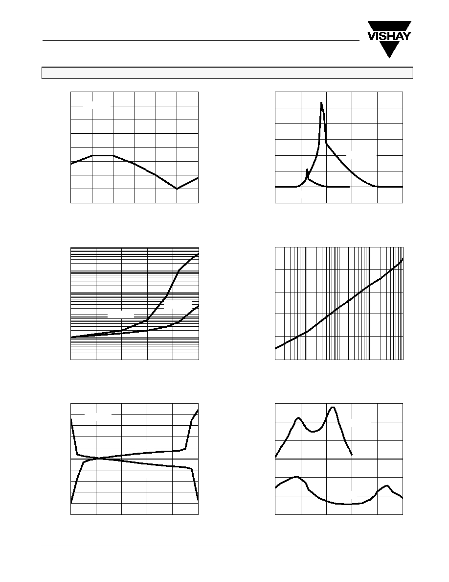
TYPICAL CHARACTERISTICS (25_C UNLESS NOTED)
�2.5
�2.0
�1.5
�1.0
�0.5
0.0
0.5
1.0
1.5
2.0
2.5
0
1
2
3
4
5
12
15
18
21
24
27
30
0
1
2
3
4
5
25
45
65
85
105
125
�140
�120
�100
�80
�60
�40
�500
0
500
1000
1500
2000
2500
3000
0
1
2
3
4
5
�2.0
�1.5
�1.0
�0.5
0.0
0.5
1.0
1.5
2.0
0.0
0.5
1.0
1.5
2.0
2.5
3.0
Charge Injection
Supply Current vs. V
IN
Off-Leakage vs. Voltage @ 25
_
C
r
DS
vs. V
COM
Leakage Current vs. Temperature
Off-Isolation vs. Frequency
V
COM
V
IN
Frequency (Hz)
V
COM
(A)
I
COM(off)
V+ = 3 V
V+ = 3 V
V+ = 5 V
OFF-Isolation (dB)
Q
V+ = 5 V
I
SUPPL
Y
m
A)
(
Temperature (
_
C)
I
COM
I
NO/NC
(pA)
I
OFF
V+ = 5 V
V
COM
(
r
DS(on)
W
)
10 nA
1 nA
100 pA
10 pA
1 pA
0.1 pA
0.1 M
1 M
10 M
0.01 M
0.001 M
INJ
(pC)
V+ = 3 V
I
COM(on)
I
COM(off)
DG9232/9233
Vishay Siliconix
Document Number: 70837
S-05298--Rev. D, 17-Dec-01
www.vishay.com
5
TYPICAL CHARACTERISTICS (25_C UNLESS NOTED)
0
20
40
60
80
100
120
1.5
2.0
2.5
3.0
3.5
4.0
4.5
5.0
0
10
20
30
40
50
60
70
�60
�30
0
30
60
90
120
r
DS
vs. V
COM
Switching Time vs. Temperature
t
ON
/t
OFF
vs. Power Supply Voltage
V
COM
/
t
ON
V+
T
(nsec)
0
7
14
21
28
35
0.0
0.5
1.0
1.5
2.0
2.5
3.0
(nsec)
t
OFF
Temperature (
_
C)
t
OFF
t
ON
t
ON
t
OFF
85
_
C
25
_
C
40
_
C
(
r
DS(on)
W
)
0.50
0.75
1.00
1.25
1.50
1.75
2.00
2.25
2
3
4
5
6
Input Switching Point vs. Power Supply Voltage
V+
V
IN
(sw)
V+ = 3 V

DG9232/9233
Vishay Siliconix
www.vishay.com
6
Document Number: 70837
S-05298--Rev. D, 17-Dec-01
TEST CIRCUITS
FIGURE 1. Switching Time
FIGURE 2. Break-Before-Make Interval
FIGURE 3. Charge Injection
C
L
(includes fixture and stray capacitance)
NO or NC
V
1
NO or NC
Switc
h
Input
C
L
(includes fixture and stray capacitance)
V+
IN
NO or NC
C
L
35 pF
COM
Logi
c
Input
R
L
300
W
V
OUT
GND
V+
50%
0 V
0 V
Logic
Input
Switch
Output
t
ON
t
OFF
Logic "1" = Switch On
Logic input waveforms inverted for switches that have
the opposite logic sense.
Off
On
On
IN
D
V
OUT
V
OUT
Q =
D
V
OUT
x C
L
C
L
COM
R
gen
V
OUT
NC or NO
3 V
IN
V
gen
GND
V+
V+
0 V
Switch Output
V
OUT
+
V
COM
R
L
R
L
)
R
ON
+ 3 V
0.9 x V
OUT
t
r
t
20 ns
t
f
t
20 ns
IN depends on switch configuration: input polarity
determined by sense of switch.
+
V
2
0 V
3 V
0 V
Logic
Input
Switch
Output
V
O
V
NC
= V
NO
t
r
<5 ns
t
f
<5 ns
90%
t
D
t
D
COM
1
V+
GND
V+
C
L
35 pF
R
L
300
W
COM
2
DG9232/9233
Vishay Siliconix
Document Number: 70837
S-05298--Rev. D, 17-Dec-01
www.vishay.com
7
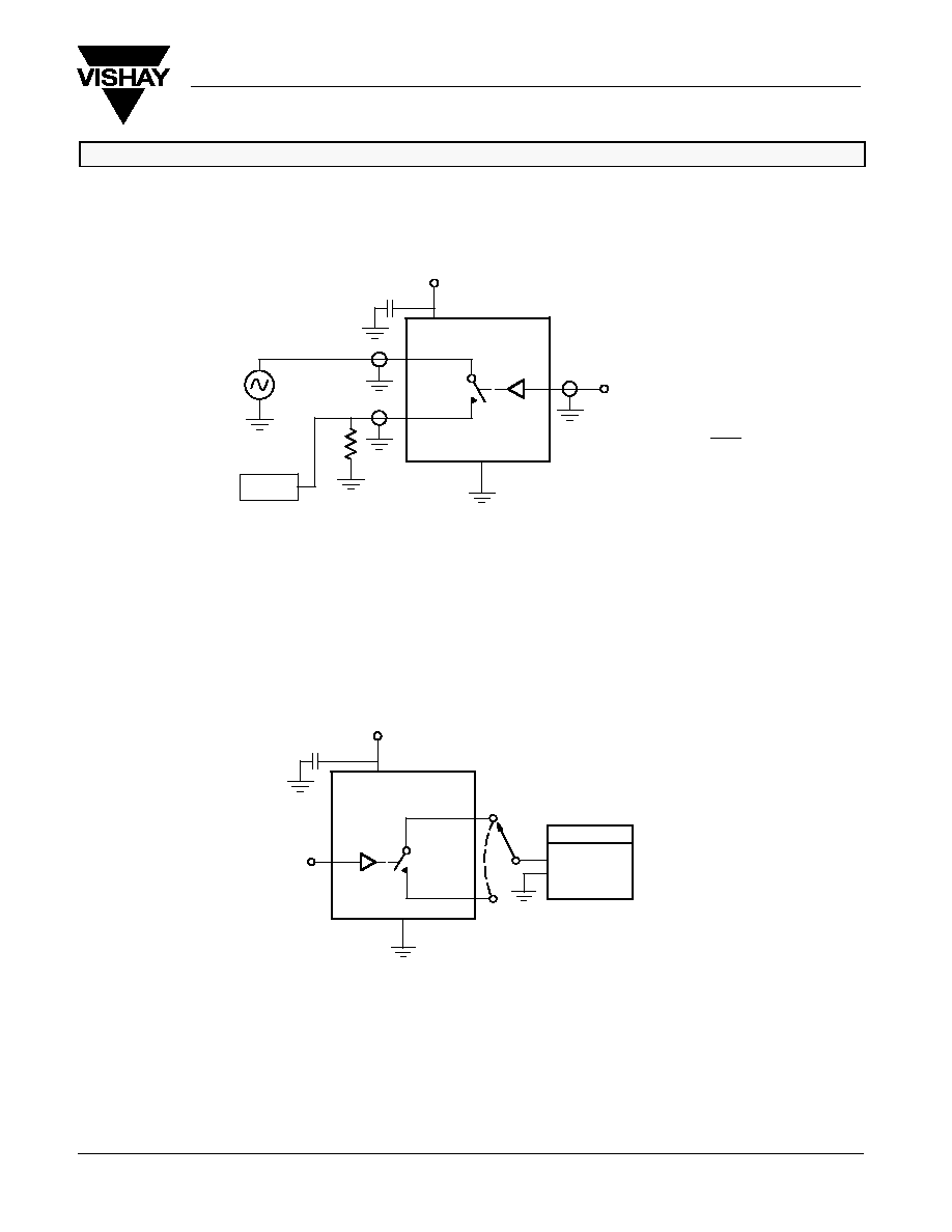
TEST CIRCUITS
FIGURE 4. Off-Isolation
FIGURE 5. Channel Off/On Capacitance
NC or NO
f = 1 MHz
IN
COM
GND
0 V, 2.4 V
Meter
HP4192A
Impedance
Analyzer
or Equivalent
10 nF
V+
V+
IN
GND
NC or NO
0V, 2.4 V
10 nF
COM
Off Isolation
+
20 log
V
NC NO
V
COM
R
L
Analyzer
V+
V+
COM