 | –≠–ª–µ–∫—Ç—Ä–æ–Ω–Ω—ã–π –∫–æ–º–ø–æ–Ω–µ–Ω—Ç: FE5C | –°–∫–∞—á–∞—Ç—å:  PDF PDF  ZIP ZIP |
VISHAY
FE5A / 5B / 5C / 5D
Document Number 86071
Rev. 1.3, 11-Aug-04
Vishay Semiconductors
www.vishay.com
1
17133
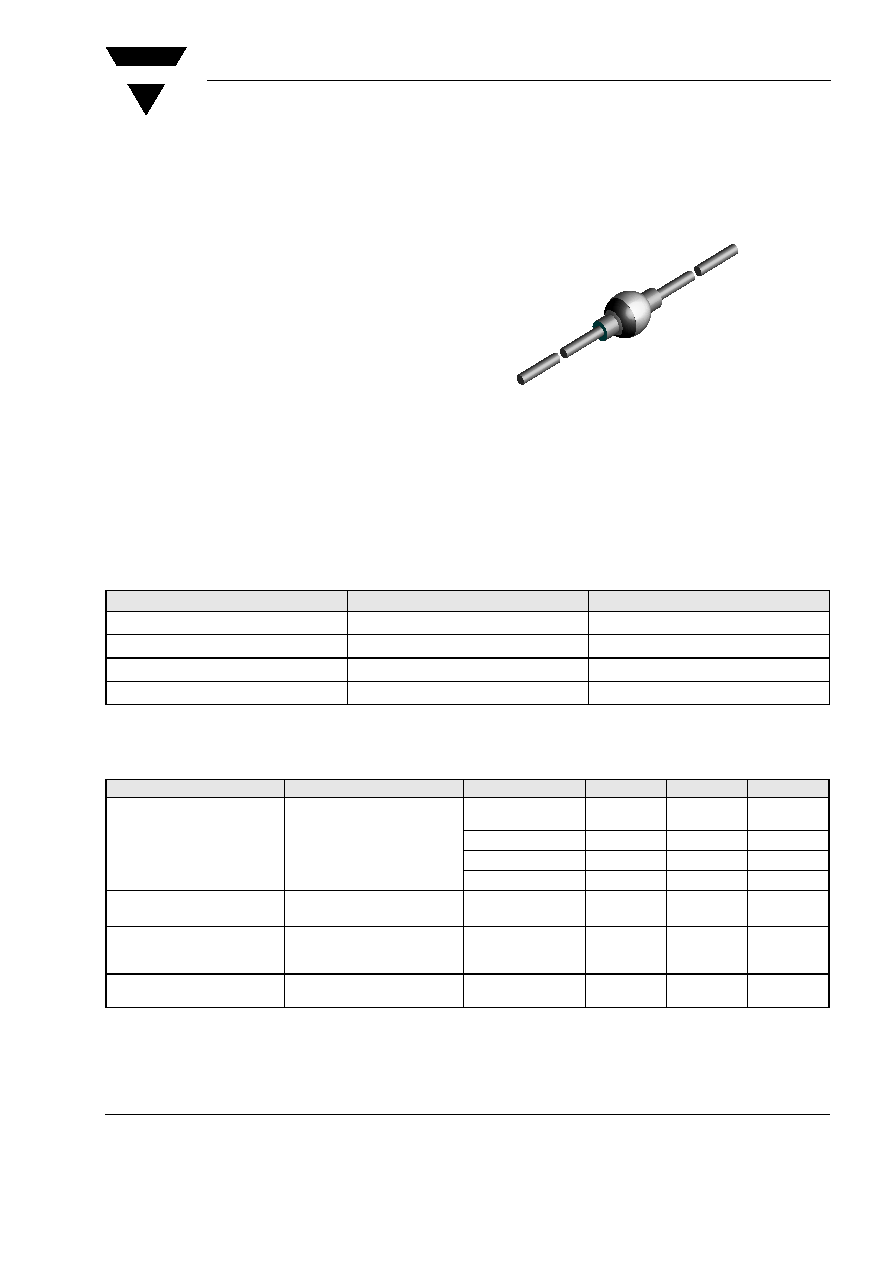
Ultra Fast Sinterglass Diode
Features
∑ High temperature metallurgically bonded con-
struction
∑ Cavity-free glass passivated junction
∑ Superfast recovery time for high efficiency
∑ Low forward voltage, high current capability
∑ Hermetically sealed package
∑ Low leakage current
∑ High surge current capability
Mechanical Data
Case: Sintered glass case, G
-4
Terminals: Plated axial leads, solderable per
MIL-STD-750, Method 2026
Polarity: Color band denotes cathode end
Mounting Position: Any
Weight: approx. 1040 mg
Parts Table
Absolute Maximum Ratings
T
amb
= 25 ∞C, unless otherwise specified
Part
Type differentiation
Package
FE5A
V
RRM
= 50 V
G-4
FE5B
V
RRM
= 100 V
G-4
FE5C
V
RRM
= 150 V
G-4
FE5D
V
RRM
= 200 V
G-4
Parameter
Test condition
Part
Symbol
Value
Unit
Reverse voltage = Repetitive
peak reverse voltage
see electrical characteristics
FE5A
V
R
= V
RRM
50
V
FE5B
V
R
= V
RRM
100
V
FE5C
V
R
= V
RRM
150
V
FE5D
V
R
= V
RRM
200
V
Maximum average forward
rectified current
0.375 " (9.5 mm) lead length at
T
L
= 55 ∞C
I
F(AV)
5.0
A
Peak forward surge current
8.3 ms single half sine-wave
superimposed on rated load
(JEDEC Method)
I
FSM
135
A
Operating junction and storage
temperature range
T
J
, T
STG
- 55 to + 175
∞C
www.vishay.com
2
Document Number 86071
Rev. 1.3, 11-Aug-04
VISHAY
FE5A / 5B / 5C / 5D
Vishay Semiconductors
Maximum Thermal Resistance
T
amb
= 25 ∞C, unless otherwise specified
1)
Thermal resistance from junction to lead 0.375 " (9.5 mm) lead length with both leads attached to heatsinks.
2)
Thermal resistance from junction to ambient at 0.375 " (9.5 mm) lead length and mounted on P.C.B.
Electrical Characteristics
T
amb
= 25 ∞C, unless otherwise specified
Typical Characteristics
(T
amb
= 25
∞C unless otherwise specified)
Parameter
Test condition
Symbol
Value
Unit
Typical thermal resistance
1), 2)
R
JA
60
K/W
R
JL
20
K/W
Parameter
Test condition
Symbol
Min
Typ.
Max
Unit
Maximum instantaneous
forward voltage
I
F
= 5.0 A
V
F
0.95
V
Maximum reverse current
V
R
= V
RRM
, T
amb
= 25 ∞C
I
R
5.0
µA
V
R
= V
RRM
, T
amb
= 100 ∞C
I
R
50
µA
Maximum reverse recovery time I
F
= 0.5 A, I
R
= 1.0 A, I
rr
= 0.25 A
t
rr
35
ns
Typical junction capacitance
V
R
= 4 V, f = 1 MHz
C
j
100
pF
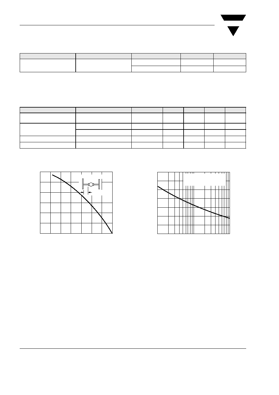
Figure 1. Maximum Forward Current Derating Curve
0
6.0
0
25
50
75
100
125
150
175
A
verage
Forward
Rectified
Current
(A)
Ambient Temperature (
∞C)
4.0
2.0
Resistive or Inductive Load
0.375" (9.5mm)
L
gfe5a_01
Figure 2. Maximum Non-Repetitive Peak Forward Surge Current
0
25
50
75
100
125
150
175
1
100
10
Peak
Forward
Surge
Current
(A)
Number of Cycles at 60 H
Z
T
J
= T
J
max.
8.3ms Single Half Sine-W ave
(JEDEC Method)
gfe5a_02
VISHAY
FE5A / 5B / 5C / 5D
Document Number 86071
Rev. 1.3, 11-Aug-04
Vishay Semiconductors
www.vishay.com
3
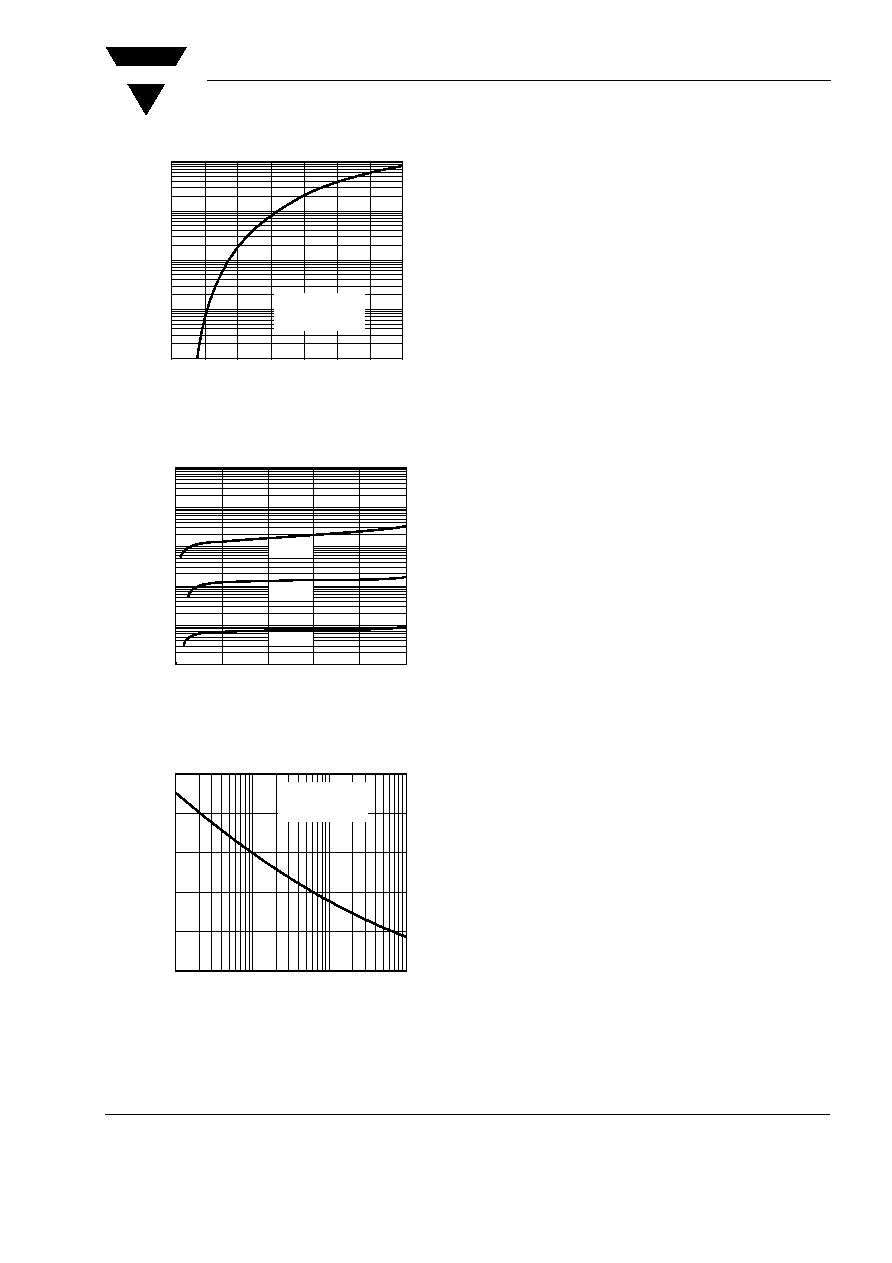
Figure 3. Typical Instantaneous Forward Characteristics
Figure 4. Typical Reverse Leakage Characteristics
Figure 5. Typical Junction Capacitance
0.4
0.6
0.8
1.0
1.2
1.4
1.6
Instantaneous Forward Voltage (V)
0.01
0.1
10
100
1
Instantaneous
Forward
Current
(A)
1.8
T
J
= 25
∞C
Pulse Width = 300
µs
1% Duty Cycle
gfe5a_03
0
20
60
40
100
80
Instantaneous
Reverse
Leakage
Current
(
µ
A)
Percent of Rated Peak Reverse Voltage (%)
T
J
= 25
∞C
T
J
= 100
∞C
T
J
= 125
∞C
0.01
0.1
10
1
100
1,000
gfe5a_04
Reverse Voltage (V)
Junction
Capacitance
(pF)
0.1
1
10
100
100
50
150
200
250
0
T
J
= 25∞C
f = 1.0 MH
Z
Vsig = 50mVp-p
gfe5a_05
www.vishay.com
4
Document Number 86071
Rev. 1.3, 11-Aug-04
VISHAY
FE5A / 5B / 5C / 5D
Vishay Semiconductors
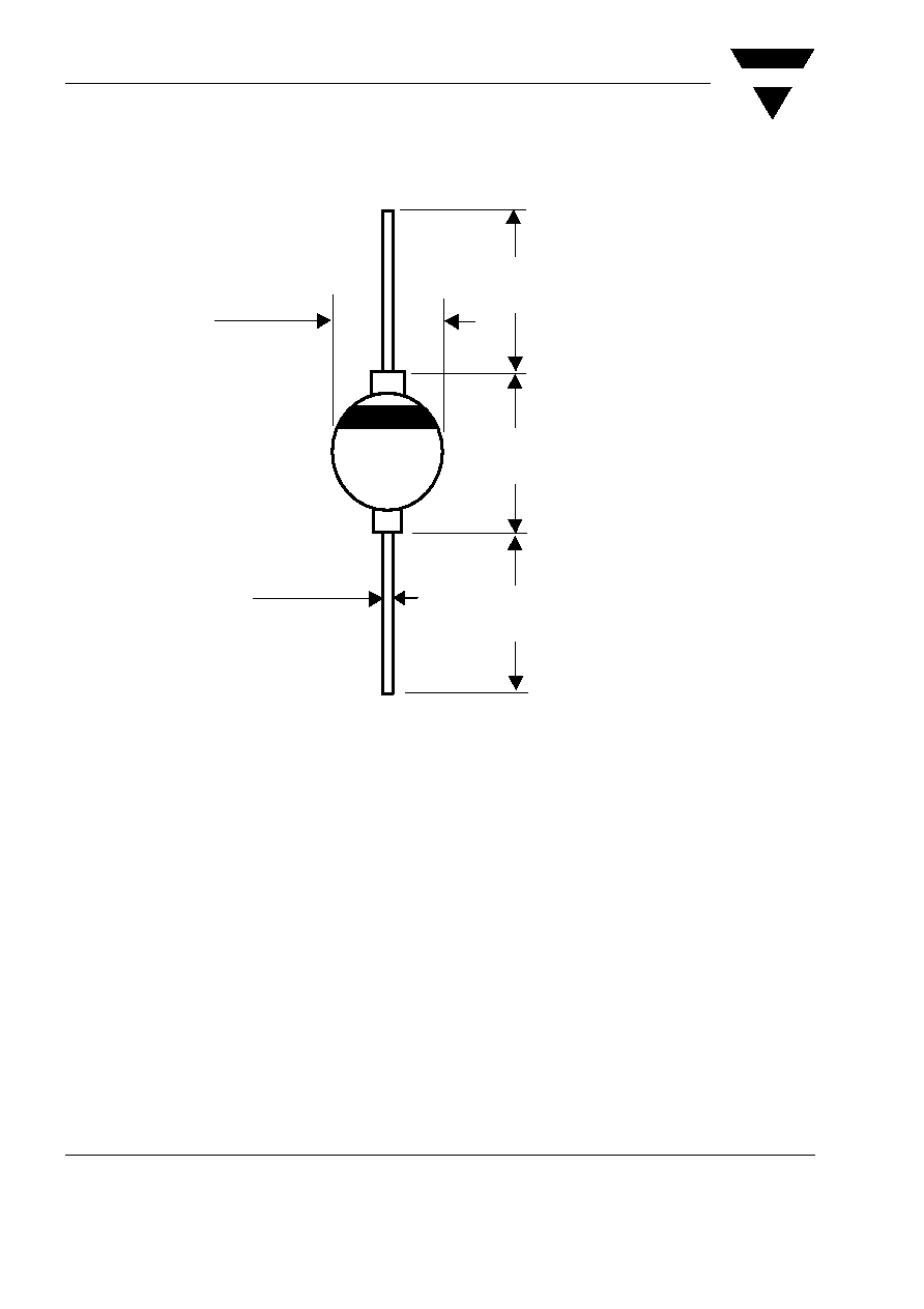
Package Dimensions in mm (Inches)
4.6 (0.180)
2.9 (0.115)
1.07 (0.042)
0.962 (0.038)
DIA.
DIA.
MAX.
7.6 (0.300)
25.4 (1.0)
MIN.
25.4 (1.0)
MIN.
17032

VISHAY
FE5A / 5B / 5C / 5D
Document Number 86071
Rev. 1.3, 11-Aug-04
Vishay Semiconductors
www.vishay.com
5
Ozone Depleting Substances Policy Statement
It is the policy of Vishay Semiconductor GmbH to
1. Meet all present and future national and international statutory requirements.
2. Regularly and continuously improve the performance of our products, processes, distribution and
operatingsystems with respect to their impact on the health and safety of our employees and the public, as
well as their impact on the environment.
It is particular concern to control or eliminate releases of those substances into the atmosphere which are
known as ozone depleting substances (ODSs).
The Montreal Protocol (1987) and its London Amendments (1990) intend to severely restrict the use of ODSs
and forbid their use within the next ten years. Various national and international initiatives are pressing for an
earlier ban on these substances.
Vishay Semiconductor GmbH has been able to use its policy of continuous improvements to eliminate the
use of ODSs listed in the following documents.
1. Annex A, B and list of transitional substances of the Montreal Protocol and the London Amendments
respectively
2. Class I and II ozone depleting substances in the Clean Air Act Amendments of 1990 by the Environmental
Protection Agency (EPA) in the USA
3. Council Decision 88/540/EEC and 91/690/EEC Annex A, B and C (transitional substances) respectively.
Vishay Semiconductor GmbH can certify that our semiconductors are not manufactured with ozone depleting
substances and do not contain such substances.
We reserve the right to make changes to improve technical design
and may do so without further notice.
Parameters can vary in different applications. All operating parameters must be validated for each
customer application by the customer. Should the buyer use Vishay Semiconductors products for any
unintended or unauthorized application, the buyer shall indemnify Vishay Semiconductors against all
claims, costs, damages, and expenses, arising out of, directly or indirectly, any claim of personal
damage, injury or death associated with such unintended or unauthorized use.
Vishay Semiconductor GmbH, P.O.B. 3535, D-74025 Heilbronn, Germany
Telephone: 49 (0)7131 67 2831, Fax number: 49 (0)7131 67 2423

Legal Disclaimer Notice
Vishay
Document Number: 91000
www.vishay.com
Revision: 08-Apr-05
1
Notice
Specifications of the products displayed herein are subject to change without notice. Vishay Intertechnology, Inc.,
or anyone on its behalf, assumes no responsibility or liability for any errors or inaccuracies.
Information contained herein is intended to provide a product description only. No license, express or implied, by
estoppel or otherwise, to any intellectual property rights is granted by this document. Except as provided in Vishay's
terms and conditions of sale for such products, Vishay assumes no liability whatsoever, and disclaims any express
or implied warranty, relating to sale and/or use of Vishay products including liability or warranties relating to fitness
for a particular purpose, merchantability, or infringement of any patent, copyright, or other intellectual property right.
The products shown herein are not designed for use in medical, life-saving, or life-sustaining applications.
Customers using or selling these products for use in such applications do so at their own risk and agree to fully
indemnify Vishay for any damages resulting from such improper use or sale.