 | –≠–ª–µ–∫—Ç—Ä–æ–Ω–Ω—ã–π –∫–æ–º–ø–æ–Ω–µ–Ω—Ç: H11D1X007 | –°–∫–∞—á–∞—Ç—å:  PDF PDF  ZIP ZIP |
H11D1/ H11D2/ H11D3/ H11D4
Document Number 83611
Rev. 1.4, 26-Oct-04
Vishay Semiconductors
www.vishay.com
1
i179004
i179004
1
2
3
6
5
4
B
C
E
A
C
NC
Pb
Pb-free
e3
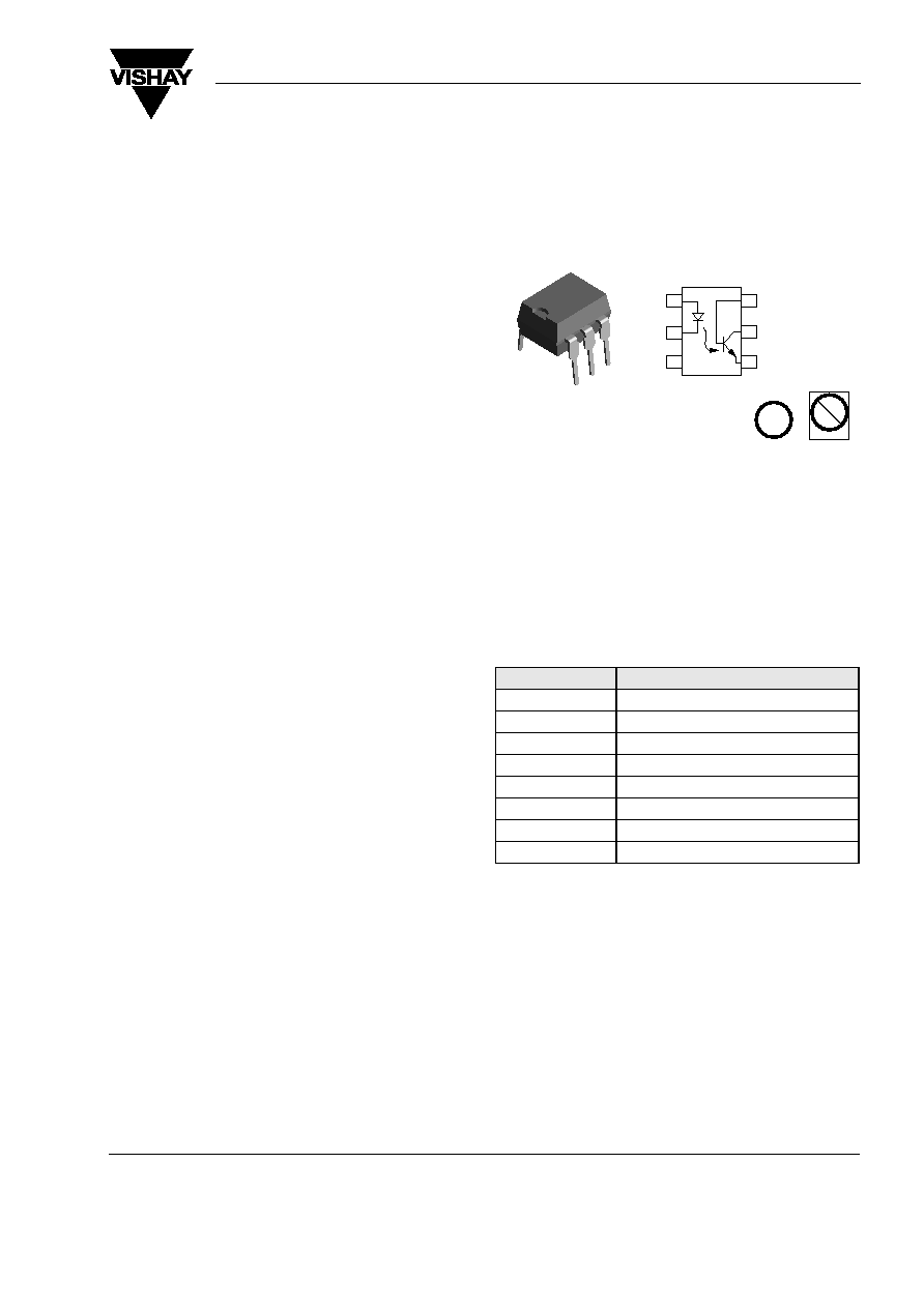
Optocoupler, Phototransistor Output, With Base Connection,
High BV
CER
Voltage
Features
∑ CTR at I
F
= 10 mA, BV
CER
= 10 V:
20 %
∑ Good CTR Linearly with Forward Current
∑ Low CTR Degradation
∑ Very High Collector-Emitter Breakdown Voltage
- H11D1/H11D2, BV
CER
= 300 V
- H11D3/H11D4, BV
CER
= 200 V
∑ Isolation Test Voltage: 5300 V
RMS
∑ Low Coupling Capacitance
∑ High Common Mode Transient Immunity
∑ Package with Base Connection
∑ Lead-free component
∑ Component in accordance to RoHS 2002/95/EC
and WEEE 2002/96/EC
Agency Approvals
∑ UL1577, File No. E52744 System Code H or J,
Double Protection
∑ DIN EN 60747-5-2 (VDE0884)
DIN EN 60747-5-5 pending
Available with Option 1
∑ BSI IEC60950 IEC60065
∑ FIMKO
Applications
Telecommunications
Replace Relays
Description
The H11D1/ H11D2/ H11D3/ H11D4 are optocou-
plers with very high BV
CER
. They are intended for
telecommunications applications or any DC applica-
tion requiring a high blocking voltage.
The H11D1/ H11D2 are identical and the H11D3/
H11D4 are identical.
Order Information
For additional information on the available options refer to
Option Information.
Part
Remarks
H11D1
CTR > 20 %, DIP-6
H11D2
CTR > 20 %, DIP-6
H11D3
CTR > 20 %, DIP-6
H11D4
CTR > 20 %, DIP-6
H11D1-X007
CTR > 20 %, SMD-6 (option 7)
H11D1-X009
CTR > 20 %, SMD-6 (option 9)
H11D2-X007
CTR > 20 %, SMD-6 (option 7)
H11D3-X007
CTR > 20 %, SMD-6 (option 7)
www.vishay.com
2
Document Number 83611
Rev. 1.4, 26-Oct-04
H11D1/ H11D2/ H11D3/ H11D4
Vishay Semiconductors
Absolute Maximum Ratings
T
amb
= 25 ∞C, unless otherwise specified
Stresses in excess of the absolute Maximum Ratings can cause permanent damage to the device. Functional operation of the device is
not implied at these or any other conditions in excess of those given in the operational sections of this document. Exposure to absolute
Maximum Rating for extended periods of the time can adversely affect reliability.
Input
Output
Coupler
Parameter
Test condition
Symbol
Value
Unit
Reverse voltage
V
R
6.0
V
DC forward current
I
F
60
mA
Surge forward current
t
10 µs
I
FSM
2.5
A
Power dissipation
P
diss
100
mW
Parameter
Test condition
Part
Symbol
Value
Unit
Collector-emitter voltage
H11D1
V
CE
300
V
H11D2
V
CE
300
V
H11D3
V
CE
200
V
H11D4
V
CE
200
V
Collector-base voltage
H11D1
V
CBO
300
V
H11D2
V
CBO
300
V
H11D3
V
CBO
200
V
H11D4
V
CBO
200
V
Emitter-base voltage
V
BEO
7.0
V
Collector current
I
C
100
mA
Power dissipation
P
diss
300
mW
Parameter
Test condition
Symbol
Value
Unit
Isolation test voltage (between
emitter and detector, refer to
climate DIN 50014, part 2,
Nov. 74)
V
ISO
5300
V
RMS
Insulation thickness between
emitter and detector
0.4
mm
Creepage distance
7.0
mm
Clearance distance
7.0
mm
Comparative tracking index (per
DIN IEC 112/VDE 0303, part 1)
175
Isolation resistance
V
IO
= 500 V, T
amb
= 25 ∞C
R
IO
10
12
V
IO
= 500 V, T
amb
= 100 ∞C
R
IO
10
11
Storage temperature range
T
stg
- 55 to + 150
∞C
Operating temperature range
T
amb
- 55 to + 100
∞C
Junction temperature
T
j
100
∞C
Soldering temperature
max. 10 sec., dip soldering:
distance to seating plane
1.5 mm
T
sld
260
∞C
H11D1/ H11D2/ H11D3/ H11D4
Document Number 83611
Rev. 1.4, 26-Oct-04
Vishay Semiconductors
www.vishay.com
3
Electrical Characteristics
T
amb
= 25 ∞C, unless otherwise specified
Minimum and maximum values are testing requirements. Typical values are characteristics of the device and are the result of engineering
evaluation. Typical values are for information only and are not part of the testing requirements.
Input
Output
Coupler
Current Transfer Ratio
Parameter
Test condition
Symbol
Min
Typ.
Max
Unit
Forward voltage
I
F
= 10 mA
V
F
1.1
1.5
V
Reverse voltage
I
R
= 10
µA
V
R
6.0
V
Reverse current
V
R
= 6.0 V
I
R
0.01
10
µA
Capacitance
V
R
= 0 V, f = 1.0 MHz
C
O
25
pF
Thermal resistance
R
thja
750
K/W
Parameter
Test condition
Part
Symbol
Min
Typ.
Max
Unit
Collector-emitter breakdown
voltage
I
CE
= 1.0 mA, R
BE
= 1.0 M
H11D1
BV
CER
300
V
H11D2
BV
CER
300
V
H11D3
BV
CER
200
V
H11D4
BV
CER
200
V
Emitter-base breakdown
voltage
I
EB
= 100
µA
BV
EBO
7.0
V
Collector-emitter capacitance
V
CE
= 10 V, f = 1.0 MHz
C
CE
7.0
pF
Collector - base capacitance
V
CB
= 10 V, f = 1.0 MHz
C
CB
8.0
pF
Emitter - base capacitance
V
EB
= 5.0 V, f = 1.0 MHz
C
EB
38
pF
Thermal resistance
R
th
250
K/W
Parameter
Test condition
Part
Symbol
Min
Typ.
Max
Unit
Coupling capacitance
C
C
0.6
pF
Current Transfer Ratio
I
F
= 10 mA, V
CE
= 10 V,
R
BE
= 1.0 M
I
C
/I
F
20
%
Collector-emitter, saturation
voltage
I
F
= 10 mA, I
C
= 0.5 mA,
R
BE
= 1.0 M
V
CEsat
0.25
0.4
V
Collector-emitter leakage
current
V
CE
= 200 V, R
BE
= 1.0 M
H11D1
I
CER
100
nA
H11D2
I
CER
100
nA
V
CE
= 300 V, R
BE
= 1.0 M
,
T
A
= 100 ∞C
H11D1
I
CER
250
µA
H11D2
I
CER
250
µA
Parameter
Test condition
Symbol
Min
Typ.
Max
Unit
Current Transfer Ratio
I
F
= 10 mA, V
CE
= 10 V,
R
BE
= 1.0 M
CTR
20
%
www.vishay.com
4
Document Number 83611
Rev. 1.4, 26-Oct-04
H11D1/ H11D2/ H11D3/ H11D4
Vishay Semiconductors
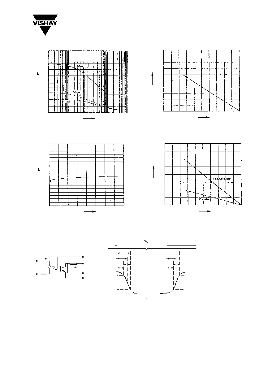
Switching Characteristics
Switching times measurement-test circuit and waveforms
Typical Characteristics (Tamb = 25
∞C unless otherwise specified)
Parameter
Test condition
Symbol
Min
Typ.
Max
Unit
Turn-on time
I
C
= 2.0 mA (to be adjusted by varying I
F
),
R
L
= 100
, V
CC
= 10 V
t
on
5.0
µs
Rise time
I
C
= 2.0 mA (to be adjusted by varying I
F
),
R
L
= 100
, V
CC
= 10 V
t
r
2.5
µs
Turn-off time
I
C
= 2.0 mA (to be adjusted by varying I
F
),
R
L
= 100
, V
CC
= 10 V
t
off
6.0
µs
Fall time
I
C
= 2.0 mA (to be adjusted by varying I
F
),
R
L
= 100
, V
CC
= 10 V
t
f
5.5
µs
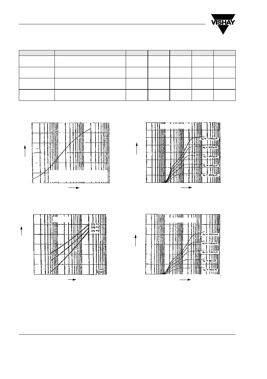
Figure 1. Current Transfer Ratio (typ.)
Figure 2. Diode Forward Voltage (typ.)
VCE =10 V,
normalized to IF = 10 mA,
NCTR = f (IF)
ih11d1_02
NTCR
1.2
1
0.8
0.6
0.4
0.2
0
10-4
10-3
10-2
10-1
IF /A
ih11d1_03
VF = f (IF, TA)
V
F
/V
0.9
1.2
V
1.1
1.0
10 -1
5
10
0
5
10 1
5 mA 10
2
I F /mA
Figure 3. Output Characteristics
Figure 4. Output Characteristics
ih11d1_04
ICE = f (VCE, IB)
I CE
/mA
100
101
102
10-2
10-1
VCE /V
20
17.5
15
12.5
10
7.5
5
2.5
0
ih11d1_05
ICE = f (VCE, IF)
I CE
/mA
100
101
102
10-2
10-1
VCE /V
20
15
10
5
0
25
30
H11D1/ H11D2/ H11D3/ H11D4
Document Number 83611
Rev. 1.4, 26-Oct-04
Vishay Semiconductors
www.vishay.com
5
Figure 5. Transistor Capacitances (typ.)
Figure 6. Collector-Emitter Leakage Current (typ.)
ih11d1_06
f=1.0 MHz,
CCE=f (VCE)
CCB=f (VCB), CEB=f (VEB)
C
XX
/pF
100
101
102
10-2
10-1
VXX /V
20
10
0
30
40
50
60
70
80
90
100
ih11d1_07
IF=0, RBE=1.0 M,
ICER=f(VCE)
C
CER
/A
VCE /V
0
25
50
75
100
125
150
175
200
10
10
10
10
10
10
10
-6
-7
-8
-9
-10
-11
-12
Figure 7. Permissible Loss Diode
Figure 8. Permissible Power Dissipation
ih11d1_08
IF = f (TA)
I F
/mA
TA /∞C
0
10
20
30
40
50
60
70
80
90
100
100
90
80
70
60
50
40
30
20
10
0
ih11d1_09
Ptot = f (TA)
P
tot
/mW
TA /∞C
0
10
20
30
40
50
60
70
80
90
100
400
350
300
250
200
150
100
50
0
Figure 9. Switching Times Measurement-Test Circuit and Waveform
ih11d1 _01
t
off
t
r
10%
50%
90%
t
s
t
pdoff
t
pdon
t
on
t
r
t
d
Output
Input
10%
50%
90%
0
0
I
F
R
L
I
C
V
O
V
CC
GND
47