 | –≠–ª–µ–∫—Ç—Ä–æ–Ω–Ω—ã–π –∫–æ–º–ø–æ–Ω–µ–Ω—Ç: J106 | –°–∫–∞—á–∞—Ç—å:  PDF PDF  ZIP ZIP |
J105/106/107
Vishay Siliconix
Document Number: 70230
S-04028--Rev. D, 04-Jun-01
www.vishay.com
7-1
N-Channel JFETs
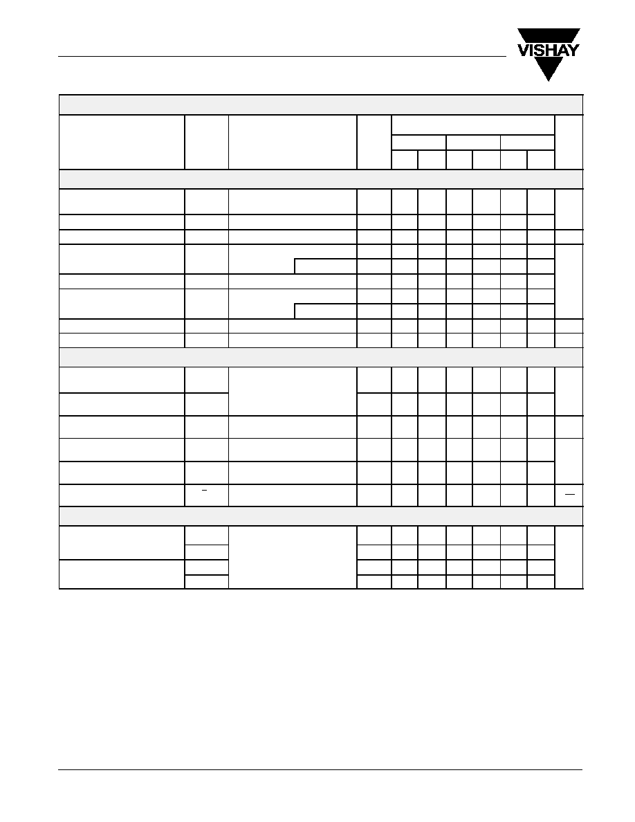
PRODUCT SUMMARY
Part Number
V
GS(off)
(V)
r
DS(on)
Max (
W
)
I
D(off)
Typ (pA)
t
ON
Typ (ns)
J105
≠4.5 to ≠10
3
10
14
J106
≠2 to ≠6
6
10
14
J107
≠0.5 to ≠4.5
8
10
14
FEATURES
BENEFITS
APPLICATIONS
D
Low On-Resistance: J105 < 3
W
D
Fast Switching--t
ON
: 14 ns
D
Low Leakage: 10 pA
D
Low Capacitance: 20 pF
D
Low Insertion Loss
D
Low Error Voltage
D
High-Speed Analog Circuit Performance
D
Negligible "Off-Error," Excellent Accuracy
D
Good Frequency Response
D
Eliminates Additional Buffering
D
Analog Switches
D
Choppers
D
Sample-and-Hold
D
Normally "On" Switches
D
Current Limiters
DESCRIPTION
The J105/106/107 are high-performance JFET analog
switches designed to offer low on-resistance and fast
switching. r
DS(on)
<3
W
is guaranteed for the J105 making this
device the lowest of any commercially available JFET.
The low cost TO-226AA (TO-92) plastic package is available
in a wide range of tape-and-reel options (see Packaging
Information). For similar products in TO-206AC (TO-52)
packaging, see the U290/291 data sheet.
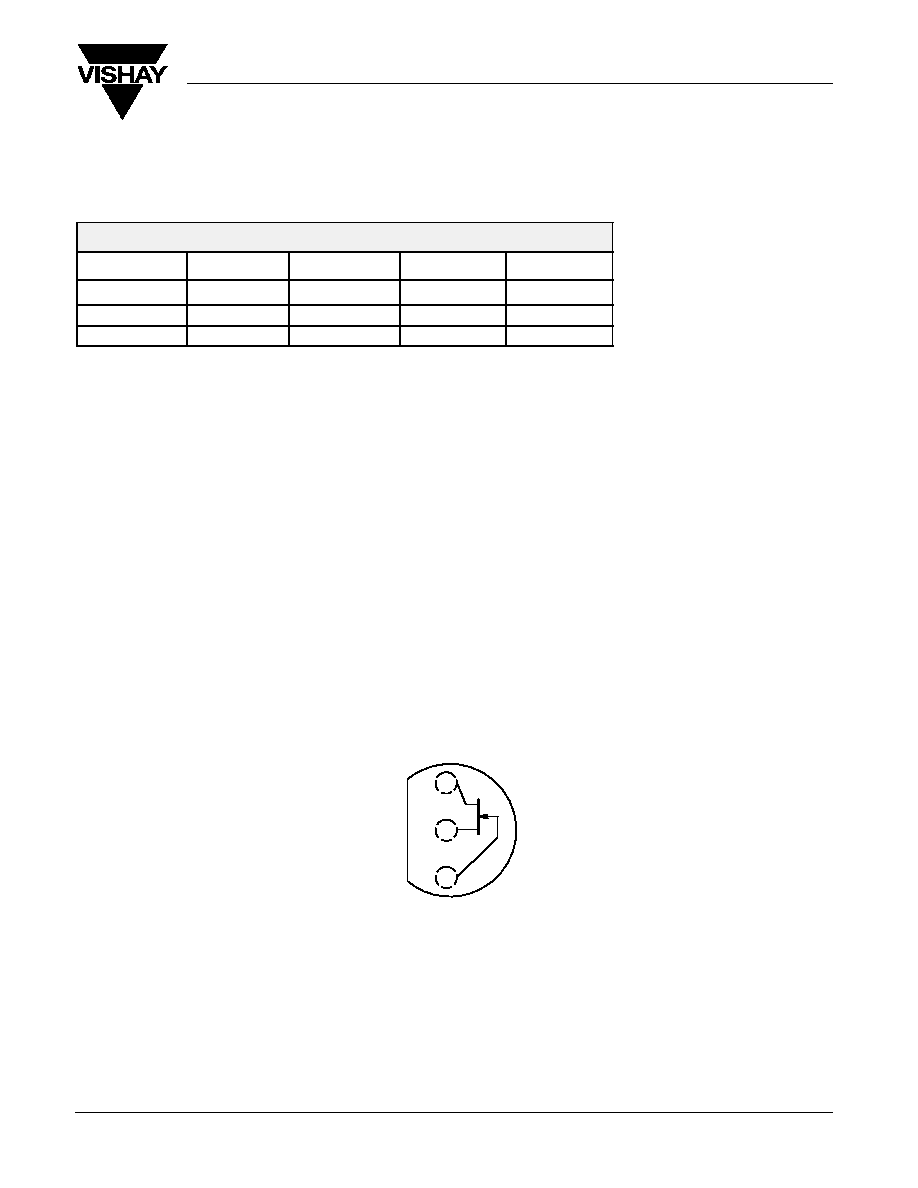
TO-226AA
(TO-92)
Top View
D
G
S
1
2
3
ABSOLUTE MAXIMUM RATINGS
Gate-Drain, Gate-Source Voltage
≠25 V
. . . . . . . . . . . . . . . . . . . . . . . . . . . . . . .
Gate Current
50 mA
. . . . . . . . . . . . . . . . . . . . . . . . . . . . . . . . . . . . . . . . . . . . . . . . .
Storage Temperature
≠55 to 150
_
C
. . . . . . . . . . . . . . . . . . . . . . . . . . . . . . . . . . .
Operating Junction Temperature
≠55 to 150
_
C
. . . . . . . . . . . . . . . . . . . . . . . . . .
Power Dissipation
a
350 mW
. . . . . . . . . . . . . . . . . . . . . . . . . . . . . . . . . . . . . . . . .
Notes
a.
Derate 2.8 mW/
_
C above 25
_
C
J105/106/107
Vishay Siliconix
www.vishay.com
7-2
Document Number: 70230
S-04028--Rev. D, 04-Jun-01
SPECIFICATIONS (T
A
= 25_C UNLESS OTHERWISE NOTED)
Limits
J105
J106
J107
Parameter
Symbol
Test Conditions
Typ
a
Min
Max
Min
Max
Min
Max
Unit
Static
Gate-Source
Breakdown Voltage
V
(BR)GSS
I
G
= ≠1
m
A , V
DS
= 0 V
≠35
≠25
≠25
≠25
V
Gate-Source Cutoff Voltage
V
GS(off)
V
DS
= 5 V, I
D
= 1
m
A
≠4.5
≠10
≠2
≠6
≠0.5
≠4.5
V
Saturation Drain Current
b
I
DSS
V
DS
= 15 V, V
GS
= 0 V
500
200
100
mA
V
GS
= ≠15 V, V
DS
= 0 V
≠0.02
≠3
≠3
≠3
Gate Reverse Current
I
GSS
T
A
= 125
_
C
≠10
Gate Operating Current
b
I
G
V
DG
= 10 V, I
D
= 25 mA
≠0.01
nA
V
DS
= 5 V, V
GS
= ≠10 V
0.01
3
3
3
Drain Cutoff Current
I
D(off)
T
A
= 125
_
C
5
Drain-Source On-Resistance
r
DS(on)
V
GS
= 0 V, I
D
= 1 mA
3
6
8
W
Gate-Source Forward Voltage
V
GS(F)
I
G
= 1 mA , V
DS
= 0 V
0.7
V
Dynamic
Common-Source Forward
Transconductance
b
g
fs
V
DS
= 10 V, I
D
= 25 mA
55
Common-Source
Output Conductance
b
g
os
V
DS
= 10 V, I
D
= 25 mA
f = 1 kHz
5
mS
Drain-Source On-Resistance
r
ds(on)
V
GS
= 0 V, I
D
= 0 mA
f = 1 kHz
3
6
8
W
Common-Source
Input Capacitance
C
iss
V
DS
= 0 V, V
GS
= 0 V
f = 1 MHz
120
160
160
160
Common-Source Reverse Transfer
Capacitance
C
rss
V
DS
= 0 V, V
GS
= ≠10 V
f = 1 MHz
20
35
35
35
pF
Equivalent Input
Noise Voltage
e
n
V
DG
= 10 V, I
D
= 25 mA
f = 1 kHz
3
nV
/
Hz
Switching
t
d(on)
6
Turn-On Time
t
r
V
DD
= 1.5 V, V
GS(H)
= 0 V
8
t
d(off)
V
DD
= 1.5 V, V
GS(H)
= 0 V
See Switching Diagram
5
ns
Turn-Off Time
t
f
9
Notes
a.
Typical values are for DESIGN AID ONLY, not guaranteed nor subject to production testing.
NVA
b.
Pulse test: PW
v
300
m
s duty cycle
v
3%.
J105/106/107
Vishay Siliconix
Document Number: 70230
S-04028--Rev. D, 04-Jun-01
www.vishay.com
7-3
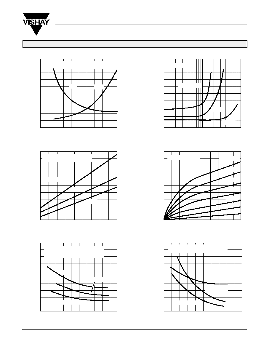
TYPICAL CHARACTERISTICS (T
A
= 25_C UNLESS OTHERWISE NOTED)
10
0
≠6
≠8
≠10
≠2
8
4
2
0
20
16
8
4
0
10
100
1000
2 .0
1.6
0
≠55
25
125
≠15
85
500
6
8
2
10
400
200
100
0
0
≠8
≠4
≠2
≠10
8
4
0
20
0
30
40
10
50
16
8
4
0
On-Resistance and Drain Current
vs. Gate-Source Cutoff Voltage
On-Resistance vs. Drain Current
Turn-On Switching
Turn-Off Switching
On-Resistance vs. Temperature
Output Characteristics
V
GS(off)
≠ Gate-Source Cutoff Voltage (V)
I
D
≠ Drain Current (mA)
T
A
≠ Temperature (
_
C)
V
DS
≠ Drain-Source Voltage (V)
V
GS(off)
≠ Gate-Source Cutoff Voltage (V)
I
D
≠ Drain Current (mA)
r
DS
@ I
D
= 10 mA, V
GS
= 0 V
I
DSS
@ V
DS
= 10 V, V
GS
= 0 V
I
DSS
r
DS
T
A
= 25
_
C
V
GS(off)
= ≠3 V
≠5 V
≠8 V
I
D
= 10 mA
r
DS
changes
X
0.7%/
_
C
t
r
approximately independent of I
D
V
DD
= 1.5 V, R
G
= 50
W
V
GS(L)
= ≠10 V
t
d(on)
@ I
D
= 10 mA
t
d(off)
V
GS(off)
= ≠8 V
V
GS(off)
= ≠3 V
t
d(off)
independent of device V
GS(off
)
V
DD
= 1.5 V, V
GS(L)
= ≠10 V
6
1.2
0.8
0.4
≠4
12
10
8
4
2
0
6
≠35
5
45
65
105
300
4
≠6
12
20
V
GS(off)
= ≠5 V
t
r
V
GS(off)
= ≠3 V
≠5 V
≠8 V
t
d(on)
@ I
D
= 30 mA
V
GS
= 0 V
≠1.0 V
≠0.5 V
≠1.5 V
≠2.0 V
≠2.5 V
≠3.0 V
t
f
Switching T
ime
(ns)
Switching T
ime
(ns)
I
D
≠
Drain Current (mA)
r
DS
(
on)
≠
Drain-Source On-Resistance (
)
r
DS
(
on)
≠
Drain-Source On-Resistance (
)
r
DS
(
on)
≠
Drain-Source On-Resistance (
)
I
DS
S
≠
Saturation Drain Current (mA)
J105/106/107
Vishay Siliconix
www.vishay.com
7-4
Document Number: 70230
S-04028--Rev. D, 04-Jun-01
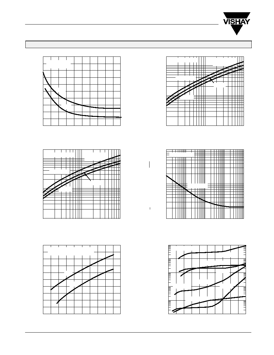
TYPICAL CHARACTERISTICS (T
A
= 25_C UNLESS OTHERWISE NOTED)
200
100
10
1
1
10
100
20
10
1
0.1
1
10
100
10
100
1 k
100 k
10 k
300
0
≠6
260
180
140
100
≠8
≠10
≠4
≠2
30
24
12
6
0
0
12
16
8
4
20
100
10
1
150
0
≠12
≠16
≠8
≠4
≠20
120
90
60
30
0
Capacitance vs. Gate-Source Voltage
Transconductance vs. Drain Current
Forward Transconductance and Output Conductance
vs. Gate-Source Cutoff Voltage
Gate Leakage Current
Output Conductance vs. Drain Current
Noise Voltage vs. Frequency
V
GS
≠ Gate-Source Voltage (V)
I
D
≠ Drain Current (mA)
I
D
≠ Drain Current (mA)
f ≠ Frequency (Hz)
V
GS(off)
≠ Gate-Source Cutoff Voltage (V)
V
DG
≠ Drain-Gate Voltage (V)
V
DS
= 0 V
f = 1 MHz
C
iss
C
rss
V
DG
= 10 V
I
D
= 10 mA
g
fs
and g
os
@ V
DS
= 10 V
V
GS
= 0 V, f = 1 kHz
g
fs
g
os
I
GSS
@ 125
_
C
I
GSS
@ 25
_
C
T
A
= 125
_
C
T
A
= 25
_
C
100 mA
100 mA
25 mA
1 pA
100 pA
10 pA
100 nA
1 nA
10 nA
V
DS
= 10 V
f = 1 kHz
T
A
= ≠55
_
C
125
_
C
T
A
= ≠55
_
C
125
_
C
220
18
25 mA
25
_
C
V
GS(off)
= ≠5 V
V
DS
= 10 V
f = 1 kHz
V
GS(off)
= ≠5 V
25
_
C
nV
e
n
/
Hz
)
(
≠
Noise V
oltage
C (pF)
g
os
≠
Output Conductance (mS)
g
os
≠
Output Conductance (mS)
I
G
≠
Gate Leakage
g
fs
≠
Forward T
ransconductance (mS)
g
os
≠
Output Conductance (mS)
g
fs
≠
Forward T
ransconductance (mS)
J105/106/107
Vishay Siliconix
Document Number: 70230
S-04028--Rev. D, 04-Jun-01
www.vishay.com
7-5
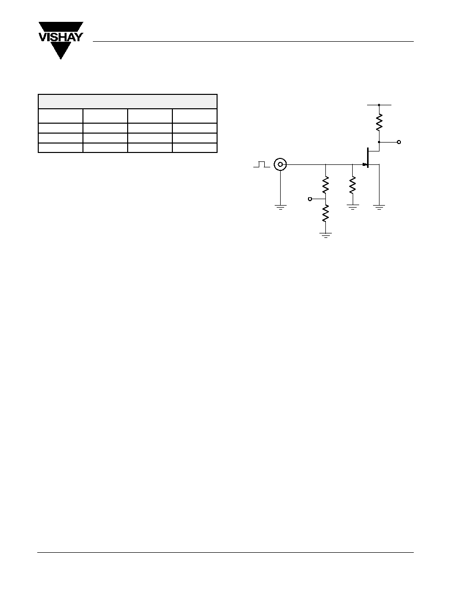
SWITCHING TIME TEST CIRCUIT
J105
J106
J107
V
GS(L)
≠12V
≠7V
≠5V
R
L
*
50 W
50 W
50 W
I
D(on)
28 mA
27 mA
26 mA
*Non-inductive
Input Pulse
Sampling Scope
Rise Time < 1 ns
Fall Time < 1 ns
Pulse Width 100 ns
PRF 1 MHz
Rise Time 0.4 ns
Input Resistance 10 M
W
Input Capacitance 1.5 pF
51
W
51
W
1 k
W
V
IN
Scope
V
DD
R
L
OUT
V
GS(H)
V
GS(L)