 | –≠–ª–µ–∫—Ç—Ä–æ–Ω–Ω—ã–π –∫–æ–º–ø–æ–Ω–µ–Ω—Ç: J204 | –°–∫–∞—á–∞—Ç—å:  PDF PDF  ZIP ZIP |
J/SST201 Series
Vishay Siliconix
Document Number: 70233
S-40393--Rev. G, 15-Mar-04
www.vishay.com
1
N-Channel JFETs
J201
SST201
J202
SST202
J204
SST204
PRODUCT SUMMARY
Part Number
V
GS(off)
(V)
V
(BR)GSS
Min (V)
g
fs
Min (mS)
I
DSS
Min (mA)
J/SST201
-0.3 to -1.5
-40
0.5
0.2
J/SST202
-0.8 to -4
-40
1
0.9
J/SST204
-0.3 to -2
-25
0.5
0.2
FEATURES
BENEFITS
APPLICATIONS
D Low Cutoff Voltage: J201 <1.5 V
D High Input Impedance
D Very Low Noise
D High Gain: A
V
= 80 @ 20 mA
D Full Performance from Low Voltage
Power Supply: Down to 1.5 V
D Low Signal Loss/System Error
D High System Sensitivity
D High Quality Low-Level Signal
Amplification
D High-Gain, Low-Noise Amplifiers
D Low-Current, Low-Voltage
Battery-Powered Amplifiers
D Infrared Detector Amplifiers
D Ultra High Input Impedance
Pre-Amplifiers
DESCRIPTION
The J/SST201 series features low leakage, very low noise,
and low cutoff voltage for use with low-level power supplies.
The J/SST201 is excellent for battery powered equipment and
low current amplifiers.
The J series, TO-226 (TO-92) plastic package, provides low
cost, while the SST series, TO-236 (SOT-23) package,
provides surface-mount capability. Both the J and SST series
are available in tape-and-reel for automated assembly (see
Packaging Information).
For similar products in TO-206AA (TO-18) packaging, see the
2N4338/4339/4340/4341 data sheet.
For applications information see AN102 and AN106.
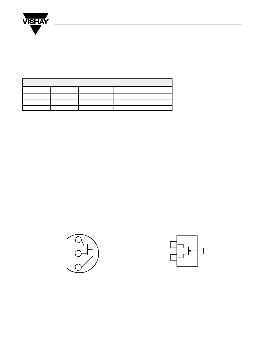
TO-226AA
(TO-92)
Top View
J201
J202
J204
D
G
S
1
2
3
D
S
G
TO-236
(SOT-23)
2
3
1
Top View
SST201 (P1)*
SST202 (P2)*
SST204 (P4)*
*Marking Code for TO-236
J/SST201 Series
Vishay Siliconix
www.vishay.com
2
Document Number: 70233
S-40393--Rev. G, 15-Mar-04
ABSOLUTE MAXIMUM RATINGS
Gate-Drain, Gate-Source Voltage
-40
V
. . . . . . . . . . . . . . . . . . . . . . . . . . . . . . .
Gate Current
50 mA
. . . . . . . . . . . . . . . . . . . . . . . . . . . . . . . . . . . . . . . . . . . . . . . . .
Lead Temperature (
1
/
16
" from case for 10 sec.)
300_C
. . . . . . . . . . . . . . . . . . .
Storage Temperature
-55 to 150_C
. . . . . . . . . . . . . . . . . . . . . . . . . . . . . . . . . . .
Operating Junction Temperature
-55 to 150_C
. . . . . . . . . . . . . . . . . . . . . . . . .
Power Dissipation
a
350 mW
. . . . . . . . . . . . . . . . . . . . . . . . . . . . . . . . . . . . . . . . .
Notes
a. Derate 2.8 mW/_C above 25_C
SPECIFICATIONS (T
A
= 25_C UNLESS OTHERWISE NOTED)
Limits
J/SST201
J/SST202
J/SST204
c
Parameter
Symbol
Test Conditions
Typ
a
Min
Max
Min
Max
Min
Max
Unit
Static
Gate-Source
Breakdown Voltage
V
(BR)GSS
I
G
= -1 mA , V
DS
= 0 V
-40
-40
-25
V
Gate-Source Cutoff Voltage
V
GS(off)
V
DS
= 15 V, I
D
= 10 nA
-0.3
-1.5
-0.8
-4
-0.3
-2
V
Saturation Drain Current
b
I
DSS
V
DS
= 15 V, V
GS
= 0 V
0.2
1
0.9
4.5
0.2
3
mA
Gate Reverse Current
I
GSS
V
GS
= -20 V, V
DS
= 0 V
-2
-100
-100
-100
pA
Gate Reverse Current
I
GSS
T
A
= 125_C
-1
nA
Gate Operating Current
I
G
V
DG
= 10 V, I
D
= 0.1 mA
-2
pA
Drain Cutoff Current
I
D(off)
V
DS
= 15 V, V
GS
= -5 V
2
pA
Gate-Source Forward Voltage
V
GS(F)
I
G
= 1 mA , V
DS
= 0 V
0.7
V
Dynamic
Common-Source
Forward Transconductance
g
fs
V
DS
= 15 V, V
GS
= 0 V
f = 1 kHz
0.5
1
0.5
mS
Common-Source
Input Capacitance
C
iss
V
DS
= 15 V, V
GS
= 0 V
4.5
pF
Common-Source
Reverse Transfer Capacitance
C
rss
V
DS
= 15 V, V
GS
= 0 V
f = 1 MHz
1.3
pF
Equivalent Input Noise Voltage
e
n
V
DS
= 10 V, V
GS
= 0 V
f = 1 kHz
6
nV/
Hz
Notes
a.
Typical values are for DESIGN AID ONLY, not guaranteed nor subject to production testing.
NPA, NH
b.
Pulse test: PW v300 ms duty cycle v3%.
c.
See 2N/SST5484 Series for J204 and SST204 typical characteristic curves.
J/SST201 Series
Vishay Siliconix
Document Number: 70233
S-40393--Rev. G, 15-Mar-04
www.vishay.com
3
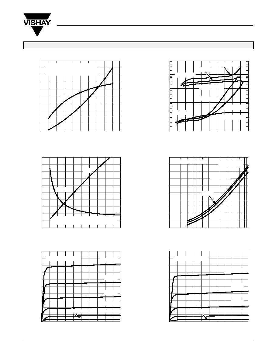
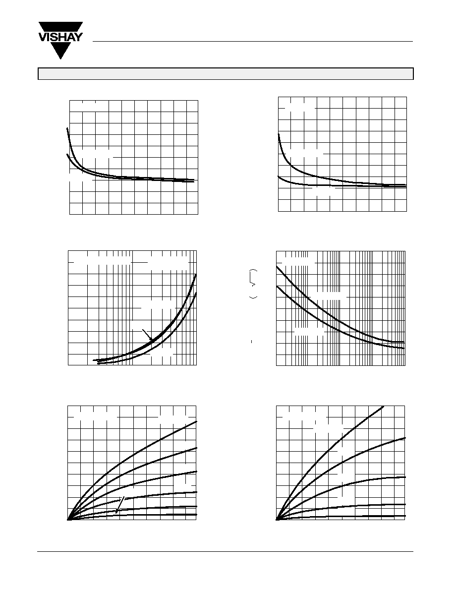
TYPICAL CHARACTERISTICS (T
A
= 25_C UNLESS OTHERWISE NOTED)
Gate Leakage Current
2
0
12
16
8
4
20
1.6
1.2
0.8
0.4
0
Output Characteristics
V
DS
- Drain-Source Voltage (V)
V
GS
= 0 V
-0.6 V
-0.9 V
-0.3 V
V
GS(off)
= -1.5 V
-1.2 V
On-Resistance and Output Conductance
vs. Gate-Source Cutoff Voltage
Drain Current and Transconductance
vs. Gate-Source Cutoff Voltage
10
0.1 pA
1 pA
10 pA
100 pA
1 nA
10 nA
0
15
30
V
DG
- Drain-Gate Voltage (V)
I
GSS
@ 125_C
I
GSS
@ 25_C
T
A
= 125_C
T
A
= 25_C
I
D
= 100 mA
I
D
= 500 mA
I
G
@ I
D
= 500 mA
I
D
= 100 mA
0
8
6
4
2
0
-5
-4
-3
-2
-1
5
4
1
3
2
0
V
GS(off)
- Gate-Source Cutoff Voltage (V)
I
DSS
@ V
DS
= 10 V, V
GS
= 0 V
g
fs
@ V
DS
= 10 V, V
GS
= 0 V
f = 1 kHz
g
fs
I
DSS
1500
0
-3
-5
-4
-2
-1
1200
900
600
300
0
0.01
0.1
1
2
1.6
0.8
0.4
0
10
8
4
2
0
400
0
12
16
4
20
360
160
80
0
Output Characteristics
Common-Source Forward Transconductance
vs. Drain Current
I
D
- Drain Current (mA)
V
GS(off)
- Gate-Source Cutoff Voltage (V)
V
DS
- Drain-Source Voltage (V)
T
A
= -55_C
125_C
-0.2 V
-0.4 V
-0.1 V
-0.3 V
r
DS
@ I
D
= 100 mA, V
GS
= 0 V
g
os
@ V
DS
= 10 V, V
GS
= 0 V, f = 1 kHz
r
DS
g
os
6
1.2
240
8
V
GS(off)
= -0.7 V
25_C
-0.5 V
V
DS
= 10 V
f = 1 kHz
V
GS(off)
= -1.5 V
V
GS
= 0 V
g
os
-
Output Conductance (
m
S)
I
DS
S
-
Saturation Drain Current (mA)
r
DS
(
on)
-
Drain-Source On-Resistance (
)
g
fs
-
Forward T
ransconductance (mS)
I
D
-
Drain Current (mA)
I
D
-
Drain Current (
m
A)
I
G
-
Gate Leakage (A)
g
fs
-
Forward T
ransconductance (mS)
J/SST201 Series
Vishay Siliconix
www.vishay.com
4
Document Number: 70233
S-40393--Rev. G, 15-Mar-04
TYPICAL CHARACTERISTICS (T
A
= 25_C UNLESS OTHERWISE NOTED)
2
0
-1.2
-1.6
-2
-0.8
-0.4
1.6
1.2
0.8
0.4
0
Transfer Characteristics
V
GS
- Gate-Source Voltage (V)
T
A
= -55_C
125_C
25_C
V
DS
= 10 V
V
GS(off)
= -1.5 V
500
0
-0.3
-0.2
-0.1
-0.4
-0.5
400
300
200
100
0
Transfer Characteristics
V
GS
- Gate-Source Voltage (V)
T
A
= -55_C
125_C
25_C
V
DS
= 10 V
V
GS(off)
= -0.7 V
0.1
1
0.01
4
-1.2
-2
-1.6
-0.8
-0.4
0
3.2
2.4
1.6
0.8
0
0.01
0.1
1
200
160
120
80
40
0
2000
1600
1200
800
400
0
I
D
- Drain Current (mA)
Circuit Voltage Gain vs. Drain Current
Transconductance vs. Gate-Source Voltage
T
A
= -55_C
125_C
V
GS
- Gate-Source Voltage (V)
On-Resistance vs. Drain Current
I
D
- Drain Current (mA)
25_C
V
GS(off)
= -0.7 V
-1.5 V
V
GS(off)
= -0.7 V
-1.5 V
1.5
0
-0.3
-0.4
-0.2
-0.1
-0.5
1.2
0.9
0.6
0.3
0
Transconductance vs. Gate-Source Voltage
T
A
= -55_C
125_C
V
GS
- Gate-Source Voltage (V)
25_C
V
DS
= 10 V
f = 1 kHz
V
GS(off)
= -0.7 V
V
DS
= 10 V
f = 1 kHz
V
GS(off)
= -1.5 V
A
V
+
g
fs
R
L
1 ) R
L
g
os
Assume V
DD
= 15 V, V
DS
= 5 V
R
L
+
10 V
I
D
g
fs
-
Forward T
ransconductance (mS)
g
fs
-
Forward T
ransconductance (mS)
r
DS
(
on)
-
Drain-Source On-Resistance (
)
I
D
-
Drain Current (mA)
I
D
-
Drain Current (
m
A)
A
V
-
V
oltage Gain
J/SST201 Series
Vishay Siliconix
Document Number: 70233
S-40393--Rev. G, 15-Mar-04
www.vishay.com
5
TYPICAL CHARACTERISTICS (T
A
= 25_C UNLESS OTHERWISE NOTED)
Common-Source Input Capacitance
vs. Gate-Source Voltage
10
0
-12
-16
-20
-8
-4
8
6
4
2
0
5
0
-12
-20
-16
-8
-4
4
3
2
1
0
Common-Source Reverse Feedback Capacitance
vs. Gate-Source Voltage
V
GS
- Gate-Source Voltage (V)
V
DS
= 0 V
10 V
f = 1 MHz
V
GS
- Gate-Source Voltage (V)
V
DS
= 0 V
10 V
f = 1 MHz
10
100
1 k
100 k
10 k
20
16
12
8
4
0
Output Conductance vs. Drain Current
I
D
- Drain Current (mA)
T
A
= -55_C
125_C
Equivalent Input Noise Voltage vs. Frequency
f - Frequency (Hz)
V
DS
= 10 V
I
D
@ 100 mA
V
GS
= 0 V
3
2.4
1.8
0.8
0.4
0
0.01
0.1
1
25_C
Output Characteristics
300
0
0.5
240
180
120
60
0
V
DS
- Drain-Source Voltage (V)
0.1
0.2
0.3
0.4
Output Characteristics
1.0
0
1.0
0.8
0.6
0.4
0.2
0
V
DS
- Drain-Source Voltage (V)
0.2
0.4
0.6
0.8
V
GS(off)
= -0.7 V
V
GS
= 0 V
-0.1
-0.2
-0.3
-0.4
-0.5
V
GS(off)
= -1.5 V
V
GS
= 0 V
-0.3
-0.6
-0.9
-1.2
V
DS
= 10 V
f = 1 kHz
V
GS(off)
= -1.5 V
e
n
-
Noise V
oltage nV
/ Hz
I
D
-
Drain Current (mA)
I
D
-
Drain Current (
µ
A)
g
os
-
Output Conductance (
µ
S)
C
is
s
-
Input Capacitance (pF)
C
rss
-
Reverse Feedback Capacitance (pF)