 | –≠–ª–µ–∫—Ç—Ä–æ–Ω–Ω—ã–π –∫–æ–º–ø–æ–Ω–µ–Ω—Ç: J511 | –°–∫–∞—á–∞—Ç—å:  PDF PDF  ZIP ZIP |
J500 Series
Vishay Siliconix
Document Number: 70196
S-04234--Rev. F, 02-Jul-01
www.vishay.com
3-1
Current Regulator Diodes
J500
J503
J506
J509
J501
J504
J507
J510
J502
J505
J508
J511
PRODUCT SUMMARY
Typ I
Typ I
Part Number
Typ I
F
(mA)
P
OV
(V)
Part Number
Typ I
F
(mA)
P
OV
(V)
J500
0.24
50
J506
1.40
50
J501
0.33
50
J507
1.80
50
J502
0.43
50
J508
2.40
50
J503
0.56
50
J509
3.00
50
J504
0.75
50
J510
3.60
50
J505
1.00
50
J511
4.70
50
FEATURES
BENEFITS
APPLICATIONS
D
Two-Lead PlasticPackage
D
Guaranteed
"
20% Tolerance
D
Operation from 1 V (J500≠J503)
to 50 V
D
Excellent Temperature Stability
D
Simple Series Circuitry, No Separate Voltage Source
D
Tight Guaranteed Circuit Performance
D
Excellent Performance in Low-Voltage/Battery
Circuits and High-Voltage Spike Protection
D
High Circuit Stability vs. Temperature
D
Constant-Current Supply
D
Current-Limiting
D
Timing Circuits
DESCRIPTION
The J500 series is a family of
"
20% range current regulators
designed for demanding applications in test equipment and
instrumentation. These devices utilize the JFET techniques to
produce a single two-leaded device which is extremely simple
to operate.
With nominal current ranges from 0.24 mA to 4.7 mA, the J500
series will meet a wide array of design requirements.
The low-cost TO-226A package ensures a cost-effective
design solution.
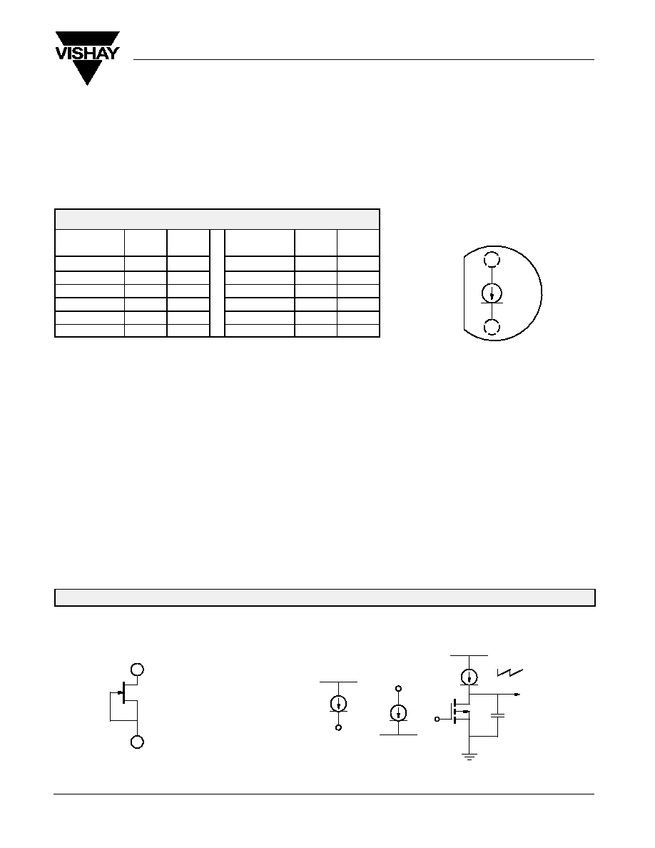
SCHEMATIC DIAGRAM
APPLICATIONS
C
A
1
2
V+
Current
Source
V≠
Current
Sink
V+
Out
Linear Ramp Generator
For applications information see AN103.
1
TO-226AA
(TO-92)
Modified
Top View
C
A
2
J500 Series
Vishay Siliconix
www.vishay.com
3-2
Document Number: 70196
S-04234--Rev. F, 02-Jul-01
ABSOLUTE MAXIMUM RATINGS
Peak Operating Voltage
50 V
. . . . . . . . . . . . . . . . . . . . . . . . . . . . . . . . . . . . . . . . .
Reverse Current
50 mA
. . . . . . . . . . . . . . . . . . . . . . . . . . . . . . . . . . . . . . . . . . . . .
Storage Temperature
≠55 to 150
_
C
. . . . . . . . . . . . . . . . . . . . . . . . . . . . . . . . . . .
Power Dissipation
a
350 mW
. . . . . . . . . . . . . . . . . . . . . . . . . . . . . . . . . . . . . . . . .
Notes:
a.
Derate 2.8 mW/
_
C above 25
_
C
SPECIFICATIONS (T
A
= 25_C UNLESS OTHERWISE NOTED)
Limits
Parameter
Symbol
Test Conditions
Min
Typ
a
Max
Unit
Peak Operating Voltage
b
P
OV
I
F
= 1.1 I
F(max)
50
95
Reverse Voltage
V
R
I
R
= 1 mA
0.8
V
Capacitance
C
F
V
F
= 25 V, f = 1 MHz
2.2
pF
Regulator
Current
c
(I
F
)
Dynamic
Impedance
d
(Z
d
)
Knee
Impedance
(Z
k
)
Limiting
Voltage
e
(V
L
)
Temperature
Coefficient
(
q
1
)
V
F
= 25 V
V
F
= 25 V
V
F
= 6 V
I
F
= 0.8 I
F(min)
V
F
= 25 V
0
_
C
v
T
A
v
100
_
C
mA
M
W
M
W
V
%/
_
C
Part Number
Min
Nom
Max
Min
Typ
a
Typ
a
Max
Typ
a
Typ
a
J500
0.192
0.24
0.288
4.00
15
2.50
1.2
0.4
0.95
J501
0.264
0.33
0.396
2.20
10
1.60
1.3
0.5
0.81
J502
0.344
0.43
0.516
1.50
7
1.10
1.5
0.6
0.70
J503
0.448
0.56
0.672
1.20
5
0.80
1.7
0.7
0.58
J504
0.600
0.75
0.900
0.80
3.5
0.55
1.9
0.8
0.46
J505
0.800
1.00
1.200
0.50
2
0.40
2.1
0.9
0.33
J506
1.120
1.40
1.680
0.33
1.5
0.25
2.5
1.1
0.19
J507
1.440
1.80
2.160
0.20
1
0.19
2.8
1.3
0.08
J508
1.900
2.40
2.900
0.20
0.7
0.13
3.1
1.5
≠0.05
J509
2.400
3.00
3.600
0.15
0.5
0.09
3.5
1.7
≠0.14
J510
2.900
3.60
4.300
0.15
0.4
0.07
3.9
1.9
≠0.22
J511
3.800
4.70
5.600
0.12
0.3
0.05
4.2
2.1
≠0.34
Notes:
NCL
a.
Typical values are for DESIGN AID ONLY, not guaranteed nor subject to production testing.
b.
Max V
F
where I
F
= 1.1 I
F(max)
is guaranteed.
c.
Pulse test--steady state currents may vary.
d.
Pulse test--steady state impedances may vary.
e.
Min V
F
required to insure I
F
= 0.8 I
F(min)
.
J500 Series
Vishay Siliconix
Document Number: 70196
S-04234--Rev. F, 02-Jul-01
www.vishay.com
3-3
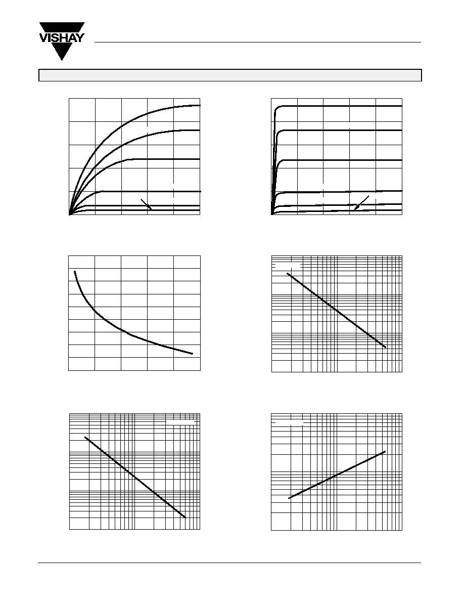
TYPICAL CHARACTERISTICS (T
A
= 25_C UNLESS OTHERWISE NOTED)
Output Current vs. Forward Voltage
Dynamic Impedance vs. Regulator Current
Limiting Voltage @ 0.8 I
F
vs. Regulator Current
Knee Impedance vs. Regulator Current
5
4
3
0
0
20
100
2
1
40
60
80
(V)
F
V
10
1
0.1
0.01
0.1
1
10
V
F
= 6 V
I
F
(mA)
100
10
1
0.1
0.1
1
10
V
F
= 25 V
I
F
(mA)
0.1
1
10
10
1
0.1
V
F
= 25 V
I
F
(mA)
Output Current vs. Forward Voltage
5
4
3
0
0
1
5
2
1
2
3
4
J502
J505
J508
J510
(V)
F
V
J511
J510
J508
J505
J502
J511
J500
J500
≠0.6
≠0.4
≠0.2
≠0.0
0.2
0.4
0.6
0.8
1.0
1.2
0
1
2
3
4
5
Temperature Coefficient
I
F
(mA)
I
F
(mA)
T
C
(%
_
C)
Z
d
(M
)
V
L
(V)
Z
k
(M
)
I
F
(mA)
J500 Series
Vishay Siliconix
www.vishay.com
3-4
Document Number: 70196
S-04234--Rev. F, 02-Jul-01
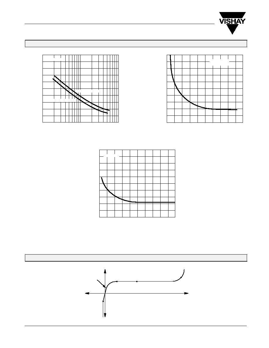
TYPICAL CHARACTERISTICS (T
A
= 25_C UNLESS OTHERWISE NOTED)
Temperature Coefficient vs. Regulator Current
On-Resistance vs. Regulator Current
Capacitance vs. Forward Voltage
0.1
1
10
0.5
≠0.5
0
T
J
= 25 to 125
_
C
T
J
= ≠55 to 25
_
C
V
F
= 25 V
2
0
1
5
1
0
I
F
(mA)
I
F
(mA)
I = 0.1 I
F
V
F
= 25 V
10
0
50
5
0
V
F
(V)
f = 1 MHz
10
20
30
40
2
3
4
T
C
(%
_
C)
r
DS
(
on)
≠
Drain-Source On-Resistance (
)
C
T
≠
T
otal Capacitance (pF)
CURRENT REGULATOR DIODE V 1 CHARACTERISTIC
Z
k
V
L
I
F
P
OV
V
R
V
R
V
F
I
F
I
R
r
DS