 | –≠–ª–µ–∫—Ç—Ä–æ–Ω–Ω—ã–π –∫–æ–º–ø–æ–Ω–µ–Ω—Ç: LH1514AAC | –°–∫–∞—á–∞—Ç—å:  PDF PDF  ZIP ZIP |

Document Number: 83814
www.vishay.com
Revision 17-August-01
3≠72
FEATURES
∑ Load Voltage, 15 V
∑ Load Current, 150 mA
∑ Switching Capability up to 50 MHz
∑ Blocking Capability Dependent upon
Signal dv/dt
∑ Low and Typical
R
ON
5.0
∑ 1.0 ms Actuation Time
∑ Low Power Consumption
∑ 3750 V
RMS
I/O Isolation
∑ Balanced Switching
∑ Linear AC/DC Operation
∑ Clean, Bounce-free Switching
∑ Surface-mountable
AGENCY APPROVALS
∑ UL ≠ File No. E52744
∑ CSA ≠ Certification 093751
∑ VDE 0884 Approval
APPLICATIONS
∑ Protection Switching (T1 sparing)
≠ Digital Access Cross Connects
≠ D-type Channel Breaks
≠ Intraoffice Data Routing
∑ Transmission Switching
≠ T1 Multiplexing
≠ DSO (64 Kbits/s)
≠ DS1 (1.544 Mbits/s)
≠ E1, DS1A (2.048 Mbits/s)
≠ DS1C (3.152 Mbits/s)
≠ DS2 (6.312 Mbits/s)
∑ Instrumentation
≠ Scanners
≠ Testers
≠ Measurement Equipment
∑ See Application Note
Part Identification
Part Number
Description
LH1514AB
8-pin DIP, Tubes
LH1514AAC
8-pin SMD, Gullwing, Tubes
LH1514AACTR
8-pin SMD, Gullwing, Tape and
Reel
DESCRIPTION
The LH1514 is a DPST normally open (2 Form A) SSR that can be
used in balanced high-frequency applications like T1 switching. With
its low ON-resistance and high actuation rate, the LH1514 is also very
attractive as a general-purpose 2 Form A SSR for balanced signals.
The relays are constructed using a GaAlAs LED for actuation control
and an integrated monolithic die for the switch output. The die, fabri-
cated in a dielectrically isolated Smart Power BiCMOS, is comprised
of a photodiode array, switch control circuitry, and NMOS switches.
In balanced switching applications, internal circuitry shunts high-fre-
quency signals between two poles when the SSR is off. This bal-
anced T termination technique provides high isolation for the load.
pin one ID
.268 (6.81)
.255 (6.48)
.390 (9.91)
.379 (9.63)
.045 (1.14)
.030 (0.76)
4
∞ typ.
.100 (2.54) typ.
10
∞
3
∞≠9∞
.300 (7.62)
typ.
.022 (.56)
.018 (.46)
.012 (.30)
.008 (.20)
.130 (3.30)
.110 (2.79)
.150 (3.81)
.130 (3.30)
.035 (.89)
.020 (.51)
.250 (6.35)
.230 (5.84)
4
3
2
1
.031 (0.79)
.050 (1.27)
5
6
7
8
Pin one I.D.
.390 (9.91)
.379 (9.63)
.045 (1.14)
.030 (0.78)
.040 (1.02)
.020 (.51)
4
∞
typ.
.008 (.25)
.004 (.10)
.150 (3.81)
.130 (3.30)
.100 (2.54)
typ.
.050
(1.27)
typ.
.312 (7.80)
.298 (7.52)
.315
(8.00)
typ.
.395 (10.03)
.375 (9.52)
.031 (.79)
typ.
.268 (6.81)
.255 (6.48)
Radius
.010
(2.54)
typ.
10
∞
3
∞
to 7
∞
Package Dimensions in Inches (mm)
DIP
SMD
8
7
6
5
S2'
S2'
S2
S2
S1
S1
S1'
S1'
1
2
3
4
LH1514AB/AAC/AACTR
2 Form A
Solid State Relay
High Frequency

Document Number: 83814
www.vishay.com
Revision 17-August-01
3≠73
Recommended Operating Conditions
Parameter
Sym.
Min.
Typ.
Max. Unit
LED Forward
Current for Switch
Turn-on
(
T
A
=≠40
∞
C to
+85
∞
C)
I
Fon
10
--
20
mA
Electrical Characteristics,
T
A
=25
∞
C
Minimum and maximum values are testing requirements. Typical values are characteristics of the device and are the result of engi-
neering evaluations. Typical values are for information purposes only and are not part of the testing requirements.
* Guaranteed by component measurement during wafer probe.
Parameter
Symbol
Min.
Typ.
Max.
Unit
Test Condition
LED Forward Current, Switch Turn-on
I
Fon
--
2.0
5.0
mA
I
L
=100 mA, t=10 ms
LED Forward Current, Switch Turn-off
I
Foff
0.2
1.8
--
mA
V
L
=±10 V
LED Forward Voltage
V
F
1.15
1.26
1.45
V
I
F
=10 mA
ON-resistance
R
ON
2.0
3.0
5.0
I
F
=10 mA,
I
L
=±50 mA
Pole-to-pole ON-resistance Matching (S1 to S2)
--
--
0.2
1.0
D
I
F
=10 mA,
I
L
=±50 mA
Output Off-state Bleed-through*
--
--
70
100
mV
peak
f=1.5 MHz square wave
t
r
/t
f
=5.0 ns
(See Figure 13.)
Output Off-state Leakage
--
--
3x10
≠12
20x10
≠12
200x10
≠9
1.0x10
≠6
A
A
I
F
=0 mA,
V
L
=
±
5.0 V
V
L
=
±
15 V
Output Off-state Leakage Pole to Pole
--
--
1.0
5.0
µ
A
I
F
=10 mA
Pins 7, 8
±
3.0 V
Pins 5, 6 Gnd
--
2.0
50
µ
A
Pins 7, 8
±
15 V
Pins 5, 6 Gnd
Output Capacitance Pins 5 to 6, 7 to 8
--
--
20
--
pF
I
F
=0 mA,
V
L
=0
Pole-to-pole Capacitance (S1 to S2)
--
--
--
20
50
--
--
pF
pF
I
F
=0 mA,
V
L
=0 V
I
F
=10 mA,
V
L
=0 V
Turn-on Time
t
on
--
0.4
1.0
ms
I
F
=10 mA,
I
L
=20 mA
Turn-off Time
t
off
--
0.6
1.0
ms
I
F
=10 mA,
I
L
=20 mA
Absolute Maximum Ratings,
T
A
=25
∞
C
Stresses in excess of the Absolute Maximum Ratings can cause permanent
damage to the device. These are absolute stress ratings only. Functional opera-
tion of the device is not implied at these or any other conditions in excess of
those given in the operational sections of the data sheet. Exposure to maximum
rating conditions for extended periods can adversely affect device reliability.
Ambient Operating Temperature Range,
T
A
.................. ≠40
∞
to +85
∞
C
Storage Temperature Range,
T
stg
................................ ≠40
∞
to +150
∞
C
Pin Soldering Temperature, t=10 s max,
T
S
................................ 260
∞
C
Input/Output Isolation Voltage,
V
ISO
.....................................3750 V
RMS
LED Input Ratings:
Continuous Forward Current,
I
F
...............................................50 mA
Reverse Voltage,
I
R
10
µ
A,
V
R
...................................................10 V
Output Operation:
dc or Peak ac Load Voltage,
I
L
1.0
µ
A,
V
L
................................15 V
Continuous dc Load Current,
I
L
Each Pole, Two Poles Operating Simultaneously .................150 mA
Power Dissipation,
P
DISS
..........................................................600 mW

Document Number: 83814
www.vishay.com
Revision 17-August-01
3≠74
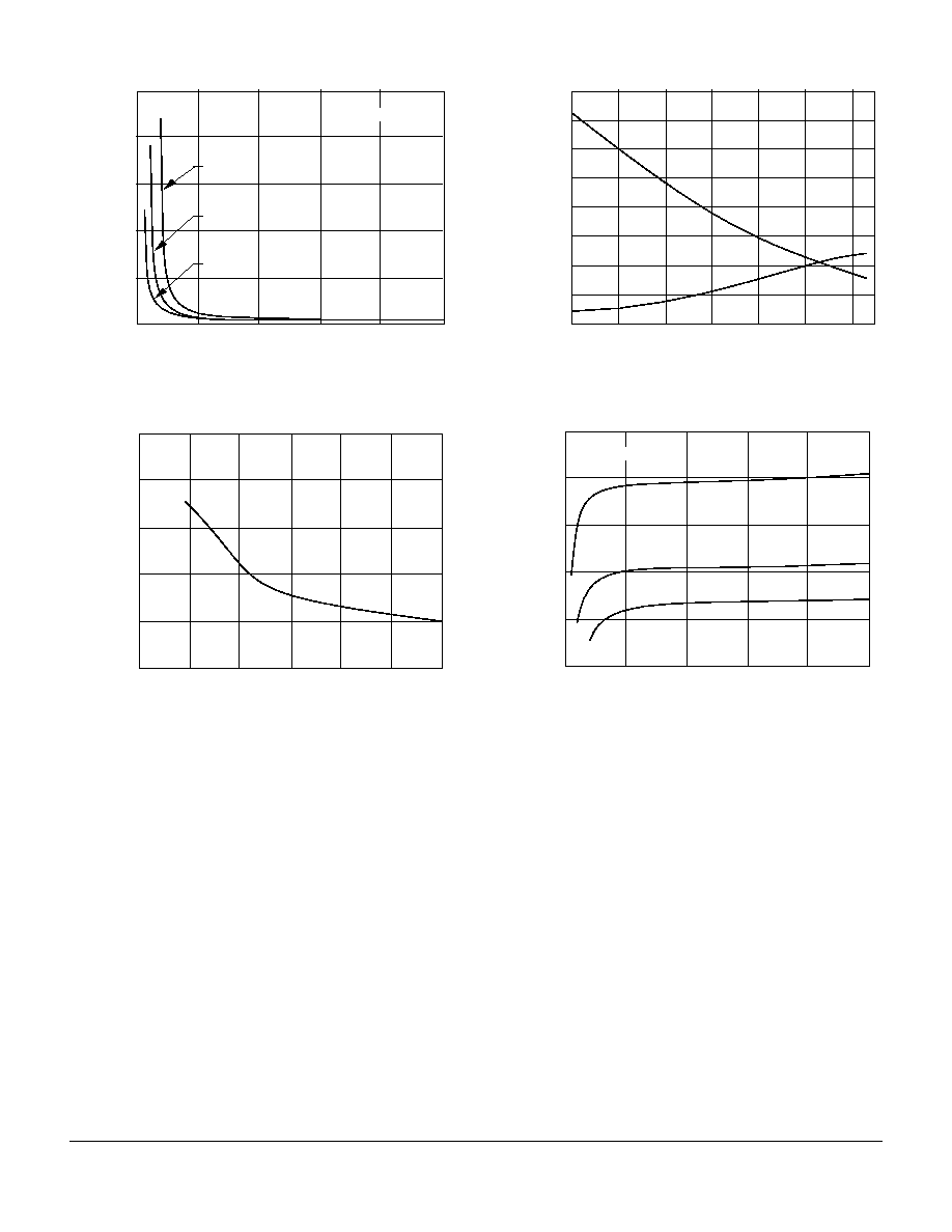
Typical Performance Characteristics
Figure 1. LED Forward Current for Switch Turn-on/off
Figure 2. Leakage Current vs. Applied Voltage
Figure 3. ON-Resistance vs. Temperature
≠40
20
Ambient Temperature (
∞C)
4.0
0.5
80
≠20
2.5
3.0
3.5
40
60
2.0
1.5
1.0
0
LED Forward Current (mA)
I
L
=100 mA
0
5
10
15
20
25
Applied Voltage (V)
0
4
8
12
16
20
Leakage Current (pA)
≠40
20
Ambient Temperature (
∞C)
8
≠6
80
≠20
2
4
6
40
60
0
≠2
≠4
0
Change in On-resistance (%)
Normalized to 25
∞
C
Figure 4. Breakdown Voltage Distribution Typical
Figure 5. Output Isolation
Figure 6. Insertion Loss (per Pole) vs. Frequency
10
20
Breakdown Voltage (V)
100
0
25
30
15
60
80
20
n=180
40
%
10
8
10
7
10
6
Frequency (Hz)
100
40
60
80
20
0
10
5
Isolation (dB)
V
P
=10 V
R
L
=50
10
8
10
6
10
4
Frequency (Hz)
0.5
0.2
0.3
0.4
0.1
0
10
2
Insertion Loss (dB)
R
L
=90
Document Number: 83814
www.vishay.com
Revision 17-August-01
3≠75
Figure 7.
t
on
vs. LED Forward Current
Figure 8.
Bleed-through Voltage vs. Rise Tim
e
0
20
10
0
50
10
4
6
8
30
40
2
≠40
∞C
25
∞C
85
∞C
LED Forward Current (mA)
Turn-on Time (ms)
I
L
=20 mA
0
10
Rise Time (ns)
100
0
15
30
5
40
60
80
20
20
25
Peak Bleedthrough Voltage (mV)
Figure 9. t
on
/t
off
vs. Temperature
Figure 10. t
off
vs. LED Forward Current
≠40
0
Ambient Temperature (
∞C)
1.1
0.3
20
80
≠20
0.8
0.9
1.0
0.4
40
60
0.5
0.6
0.7
t
off
t
on
Turn-on/off Time (ms)
0
20
LED Forward Current (mA)
1.2
0.2
30
50
40
10
0.6
0.8
1.0
0.4
≠40
∞C
25
∞C
85
∞C
Turn-off Time (ms)
I
L
=20 mA
Document Number: 83814
www.vishay.com
Revision 17-August-01
3≠76
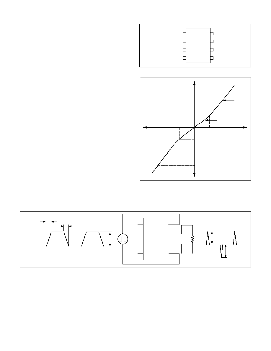
Functional Description
Figure 12 shows the switch characteristics of the relay. The
relay exhibits an ON-resistance that is exceptionally linear up
to the knee current (I
K
). Beyond I
K
, the incremental resistance
decreases, minimizing internal power dissipation.
In a 2 Form A relay, to turn the relay on, forward current is
applied to the LED. The amount of current applied determines
the amount of light produced for the photodiode array.
This photodiode array develops a drive voltage for both NMOS
switch outputs. For high-temperature or high-load current
operations, more LED current is required.
For high-frequency applications, the LH1514 must be wired as
shown in the Figure 15 application diagram to minimize trans-
mission crosstalk and bleed-through. A single LH1514 pack-
age switches a single transmit twisted pair or a single receive
twisted pair. In this configuration when the SSR is turned off,
the SSR parries high-frequency signals by shunting them
through the SSR, thereby isolating the transformer load.
When switching alternate mark inversion (AMI) coding trans-
mission, the most critical SSR parameter is dv/dt bleed-
through. This bleed-through is a result of the rise and fall time
slew rates of the 3.0 V AMI pulses. The test circuit in Figure 13
illustrates these bleed-through glitches. It is important to rec-
ognize that the transmission limitations of the LH1514 are
bleed-through related and not frequency related. The maxi-
mum frequency the LH1514 SSR can switch will be determined
by the pulse rise and fall times and the sensitivity of the receive
electronics to the resultant bleed-through.
At data rates above 2.0 Mbits/s, the 50 pF pole-to-pole capaci-
tance of the LH1514 should be considered when analyzing the
load match to the transmission line. Please refer to the T1
Switching with the LH1514 SSR Application Note for further
information on load-matching and off-state blocking.
Figure 11. Pin Diagram and Pin Outs
Figure 12. Typical ON Characteristics
1
2
3
S1
S1'
S2
CONTROL +
CONTROL +
CONTROL≠
8
7
6
DPST
4
S2'
BLANK
5
≠150 mA
150 mA
60 mA
≠60 mA
≠V
+V
+I
≠I
I
L
(max)
I
K
I
K
0.3 V
≠0.3 V
4.0
5.0
I
L
(max)
Test Circuit
Figure 13. Off-state Bleed-through
* 50
load is derived from T1 applications where a 100 load is paralleled with a 100 line.
NC
NC
NC
NC
1
2
3
4
8
7
6
5
100 mV
max
100 mV
max
50
*
tf 5.0 ns
f = 1.5 MHz
3.0 V
tr 5.0 ns