 | –≠–ª–µ–∫—Ç—Ä–æ–Ω–Ω—ã–π –∫–æ–º–ø–æ–Ω–µ–Ω—Ç: LH1518AT | –°–∫–∞—á–∞—Ç—å:  PDF PDF  ZIP ZIP |
VISHAY
LH1518AAB/ AABTR/ AT
Document Number 83816
Rev. 1.2, 08-Mar-04
Vishay Semiconductors
www.vishay.com
1
4
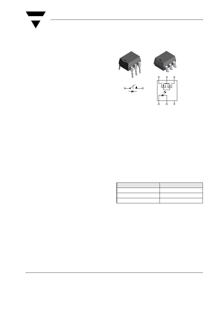
6
5
S'
S
DC
1
2
3
S
S'
i179001
DIP
SMD
1 Form A Solid State Relay
Features
∑ Isolation Test Voltage 5300 V
RMS
∑ Current-limit Protection
∑ Linear AC/DC Operation
∑ High-reliability Monolithic Detector
∑ Low Power Consumption
∑ Clean, Bounce-free Switching
∑ High Surge Capability
∑ Surface Mountable
Agency Approvals
∑ UL - File No. E52744 System Code H or J
∑ CSA - Certification 093751
∑ BSI/BABT Cert. No. 7980
∑ DIN EN 60747-5-5 (VDE 0884):2003-01 Available
with Option 1
∑ FIMKO Approval
Applications
General Telecom Switching
Instrumentation
Industrial Controls
Description
Vishay Solid State Relays (SSRs) are miniature, opti-
cally- coupled relays with high-voltage MOSFET out-
puts. The LH1518 relays are capable of switching AC
or DC loads from as little as nanovolts to hundreds of
volts.
The relays can switch currents in the range of nano-
amps to hundreds of milliamps. The MOSFET
switches are ideal for small signal switching and are
primarily suited for dc or audio frequency applica-
tions.
The LH1518 relays feature a monolithic output die
that minimizes wire bonds and permits easy integra-
tion of high-performance circuits such as current lim-
iting in normally-open switches. The output die
integrates the photodiode receptor array, turn-on and
turn-off control circuitry, and the MOSFET switches.
The optically-coupled input is controlled by a highly
efficient GaAlAs infrared LED.
Order Information
Part
Remarks
LH1518AAB
SMD-6, Tubes
LH1518AABTR
SMD-6, Tape and Reel
LH1518AT
DIP-6, Tubes

www.vishay.com
2
Document Number 83816
Rev. 1.2, 08-Mar-04
VISHAY
LH1518AAB/ AABTR/ AT
Vishay Semiconductors
Absolute Maximum Ratings, T
amb
= 25 ∞C
Stresses in excess of the absolute Maximum Ratings can cause permanent damage to the device. Functional operation of the device is
not implied at these or any other conditions in excess of those given in the operational sections of this document. Exposure to absolute
Maximum Ratings for extended periods of time can adversely affect reliability.
SSR
1)
Refer to Current Limit Performance Application Note 58 for a discussion on relay operation during transient currents.
Electrical Characteristics, T
amb
= 25 ∞C
Minimum and maximum values are testing requirements. Typical values are characteristics of the device and are the result of engineering
evaluations. Typical values are for information only and are not part of the testing requirements.
Input
Output
Parameter
Test condition
Symbol
Value
Unit
LED continuous forward current
I
F
50
mA
LED reverse voltage
I
R
10 µA
V
R
8.0
V
DC or peak AC load voltage
V
L
250
V
Continuous DC load current,
bidirectional operation
I
L
155
mA
Continuous DC load current,
unidirectional operation
I
L
300
mA
Peak load current (single shot)
t = 100 ms
I
P
1)
Ambient temperature range
T
amb
- 40 to + 85
∞C
Storage temperature range
T
stg
- 40 to + 150
∞C
Pin soldering temperature
t = 10 s max
T
sld
260
∞C
Input/output isolation voltage
V
ISO
5300
V
RMS
Output power dissipation
(continuous)
P
diss
550
mW
Parameter
Test condition
Symbol
Min
Typ.
Max
Unit
LED forward current,
switch turn-on
I
L
= 100 mA, t = 10 ms
I
Fon
0.8
2.0
mA
LED forward current,
switch turn-off
V
L
= ± 200 V
I
Foff
0.2
0.7
mA
LED forward voltage
I
F
= 10 mA
V
F
1.15
1.26
1.45
V
Parameter
Test condition
Symbol
Min
Typ.
Max
Unit
ON-resistance ac/dc:
Pin 4(±) to 6 (±)
I
F
= 5.0 mA, I
L
= 50 mA
R
ON
10
15
20
ON-resistance dc:
Pin 4, 6 (+) to 5 (±)
I
F
= 5.0 mA, I
L
= 100 mA
R
ON
2.5
3.75
5.0
Off-resistance
I
F
= 0 mA, V
L
= ± 100 V
R
OFF
0.5
5000
G
Current limit ac/dc :
Pin 4 (±) to 6 (±)
I
F
= 5.0 mA, V
L
= ± 6.0 V,
t = 5.0 ms
I
LMT
170
200
280
mA
Off-state leakage current
I
F
= 0 mA, V
L
= ± 100 V
I
O
0.02
200
nA
I
F
= 0 mA, V
L
= ± 250 V
I
O
1.0
µA
Output capacitance Pin 4 to 6
I
F
= 0 mA, V
L
= 1.0 V
C
O
55
pF
I
F
= 0 mA, V
L
= 50 V
C
O
10
pF
Switch offset
I
F
= 5.0 mA
V
OS
0.15
V
VISHAY
LH1518AAB/ AABTR/ AT
Document Number 83816
Rev. 1.2, 08-Mar-04
Vishay Semiconductors
www.vishay.com
3
Transfer
Typical Characteristics
(T
amb
= 25
∞C unless otherwise specified)
Parameter
Test condition
Symbol
Min
Typ.
Max
Unit
Capacitance (input-output)
V
ISO
= 1.0 V
C
IO
0.8
pF
Turn-on time
I
F
= 5.0 mA, I
L
= 50 mA
t
on
1.4
3.0
ms
Turn-off time
I
F
= 5.0 mA, I
L
= 50 mA
t
off
0.7
3.0
ms
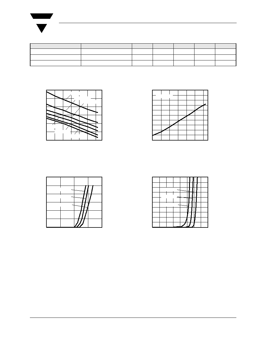
Fig. 1 LED Voltage vs. Temperature
Fig. 2 LED Forward Current vs. LED Forward Voltage
1.0
1.1
1.2
1.3
1.4
1.5
1.6
≠40
≠20
0
20
40
60
80
Temperature ( C )
17300
I
F
= 50 mA
LED Forward V
oltage ( V )
I
F
= 10 mA
I
F
= 20 mA
I
F
= 5 mA
I
F
= 1 mA
I
F
= 2 mA
0
20
40
60
80
100
120
0.0
0.5
1.0
1.5
2.0
LED Forward Voltage ( V )
17301
T = 85 C
LED Forward Current ( mA
)
T = 25 C
T = ≠40 C
Fig. 3 ON-Resistance vs. Temperature
Fig. 4 LED Reverse Current vs. LED Reverse Voltage
≠40
≠30
≠20
≠10
0
10
20
30
40
50
60
≠40
≠20
0
20
40
60
80
Ambient Temperature ( C )
17302
I
L
= 50 mA
Normalized to 25 C
Change in On≠Resistance (%)
0
1
2
3
4
5
6
7
8
9
10
0
10
20
30
40
50
60
70
80
LED Reverse Voltage ( V )
17303
T = 85 C
LED Reverse Current (
A
)
T = 25 C
T = ≠40 C
www.vishay.com
4
Document Number 83816
Rev. 1.2, 08-Mar-04
VISHAY
LH1518AAB/ AABTR/ AT
Vishay Semiconductors
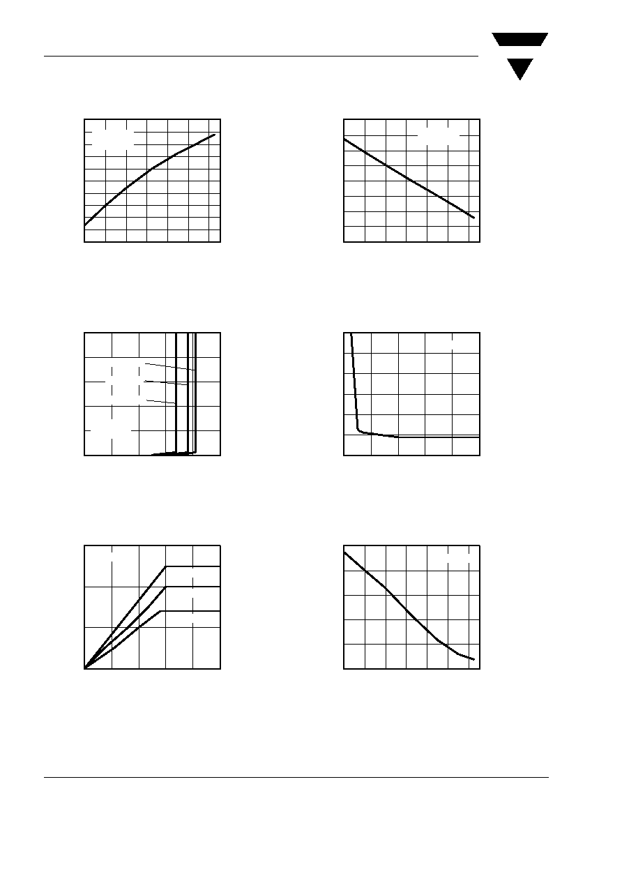
Fig. 5 Switch Breakdown Voltage vs. Temperature
Fig. 6 Switch Breakdown Voltage vs. Load Current
Fig. 7 Load Current vs. Load Voltage
≠12
≠10
≠8
≠6
≠4
≠2
0
2
4
6
8
≠40
≠20
0
20
40
60
80
Ambient Temperature ( C )
17304
I
F
= 0
I
L
t50 A
Normalized to 25 C
Change in Breakdown V
oltage ( % )
0
10
20
30
40
50
0
100
200
300
400
500
Load Voltage ( V )
17305
T = 85 C
Load Current (
A
)
T = 25 C
T = ≠40 C
I
F
= 0
I
L
t50 A
0
100
200
300
0
1
2
3
4
5
Load Voltage ( V )
17306
T = 85 C
Load Current ( mA
)
T = 25 C
T = ≠40 C
I
F
= 5 mA
Fig. 8 Current Limit vs. Temperature
Fig. 9 Variation in ON-Resistance vs. LED Current
Fig. 10 LED Dropout Voltage vs. Temperature
≠40
≠30
≠20
≠10
0
10
20
30
40
≠40
≠20
0
20
40
60
80
Ambient Temperature ( C )
17307
I
F
= 5 mA
V
L
= 6 V
Normalized to 25 C
Change in Current Linit ( % )
≠2
0
2
4
6
8
10
0
4
8
12
16
20
LED Current ( mA )
17308
I
L
= 50 mA
norm. at I = 5 mA
F
ac/dc R≠on V
ariation ( % )
1.04
1.08
1.12
1.16
1.20
1.24
≠40
≠20
0
20
40
60
80
Temperature ( C )
17309
I
L
= 100 mA
LED Dropout V
oltage ( V )

VISHAY
LH1518AAB/ AABTR/ AT
Document Number 83816
Rev. 1.2, 08-Mar-04
Vishay Semiconductors
www.vishay.com
5
Fig. 11 Insertion Loss vs. Frequency
Fig. 12 Output Isolation
Fig. 13 Switch Capacitance vs. Applied Voltage
0.00
0.05
0.10
0.15
0.20
0.25
Frequency ( Hz )
17310
R
L
= 600
Insertion Loss ( dB )
100
1000
10000
100000
0
20
40
60
80
100
120
Frequency ( Hz )
17311
R
L
= 50
V
P
= 10 V
Isolation ( dB )
1000
10000
100000
1000000
0
20
40
60
80
100
0
20
40
60
80
100
Applied Voltage ( V )
17312
I
F
= 0
Capacitance ( pF )
Fig. 14 Leakage Current vs. Applied Voltage
Fig. 15 Switch Offset Voltage vs. LED Current
Fig. 16 Switch Offset Voltage vs. Temperature
0
50
100
150
200
250
Load Voltage ( V )
17313
I
F
= 0
Leakage Current ( nA
)
T = 85 C
T = 25 C
T = 70 C
T = 50 C
1
10
100
1000
0.1
0.3
0.4
0.5
0.6
0.7
0.8
0
5
10
15
20
25
LED Current ( mA )
17314
Switch Of
fset V
oltage ( V )
0.0
0.5
1.0
1.5
2.0
2.5
3.0
25
35
45
55
65
75
85
Temperature ( C )
17315
Switch Of
fset V
oltage ( V )
I
F
= 5 mA