
FEATURES
D TrenchFETr Power MOSFET
APPLICATIONS
D Direct Logic-Level Interface: TTL/CMOS
D Drivers: Relays, Solenoids, Lamps, Hammers,
Displays, Memories, Transistors, etc.
D Battery Operated Systems
D Solid-State Relays
TN0201K/TN0201KL
Vishay Siliconix
New Product
Document Number: 72671
S-40245--Rev. A, 16-Feb-04
www.vishay.com
1
N-Channel 20-V (D-S) MOSFET
PRODUCT SUMMARY
V
(BR)DSS
r
DS(
)
I
D
(A)
V
(BR)DSS
Min (V)
r
DS(on)
Max (W)
V
GS(th)
(V)
TN0201K
TN0201KL
20
1.0 @ V
GS
= 10 V
1 0 to 3 0
0.42
0.64
20
1.4 @ V
GS
= 4.5 V
1.0 to 3.0
0.35
0.53
TO-226AA
(TO-92)
Top View
S
D
G
1
2
3
G
S
D
Top View
2
3
TO-236
(SOT-23)
1
TN0201KL
Device Marking
Front View
"S" TN
0201KL
xxyy
"S" = Siliconix Logo
xxyy = Date Code
Marking Code: K3ywl
K3 = Part Number Code for TN0201K
y = Year Code
w = Week Code
l = Lot Traceability
TN0201K
Ordering Information: TN0201K-T1--E3 (Lead Free)
Ordering Information: TN0201KL-TR1
ABSOLUTE MAXIMUM RATINGS (T
A
= 25_C UNLESS OTHERWISE NOTED)
Limit
Parameter
Symbol
TN0201K
TN0201KL
Unit
Drain-Source Voltage
V
DS
20
V
Gate-Source Voltage
V
GS
"20
V
Continuous Drain Current
(T
J
= 150_C)
T
A
= 25_C
I
D
0.42
0.64
Continuous Drain Current
(T
J
= 150_C)
T
A
= 70_C
I
D
0.33
0.51
A
Pulsed Drain Current
a
I
DM
0.8
1.5
Power Dissipation
T
A
= 25_C
P
D
0.35
0.8
W
Power Dissipation
T
A
= 70_C
P
D
0.22
0.51
W
Thermal Resistance, Junction-to-Ambient
R
thJA
357
156
_C/W
Operating Junction and Storage Temperature Range
T
J
, T
stg
-55 to 150
_C
Notes
a.
Pulse width limited by maximum junction temperature.
TN0201K/TN0201KL
Vishay Siliconix
New Product
www.vishay.com
2
Document Number: 72671
S-40245--Rev. A, 16-Feb-04
SPECIFICATIONS (T
A
= 25_C UNLESS OTHERWISE NOTED)
Limits
Parameter
Symbol
Test Conditions
Min
Typ
Max
Unit
Static
Drain-Source Breakdown Voltage
V
(BR)DSS
V
GS
= 0 V, I
D
= 10 mA
20
V
Gate-Threshold Voltage
V
GS(th)
V
DS
= V
GS
, I
D
= 0.25 mA
1.0
2.0
3.0
V
Gate-Body Leakage
I
GSS
V
DS
= 0 V, V
GS
= "20 V
"100
nA
Zero Gate Voltage Drain Current
I
DSS
V
DS
= 20 V, V
GS
= 0 V
1
mA
Zero Gate Voltage Drain Current
I
DSS
V
DS
= 20 V, V
GS
= 0 V, T
J
= 55_C
10
mA
On State Drain Current
a
I
D( )
V
DS
= 10 V V
GS
= 10 V
TN0201K
0.5
A
On-State Drain Current
a
I
D(on)
V
DS
= 10 V, V
GS
= 10 V
TN0201KL
0.8
A
Drain-Source On-Resistance
a
r
DS(on)
V
GS
= 4.5 V, I
D
= 0.1 A
0.8
1.4
W
Drain-Source On-Resistance
a
r
DS(on)
V
GS
= 10 V, I
D
= 0.3 A
0.47
1.0
W
Forward Transconductance
a
g
fs
V
DS
= 10 V, I
D
= 0.3 A
550
mS
Diode Forward Voltage
V
SD
I
S
= 0.3 A, V
GS
= 0 V
0.85
1.2
V
Dynamic
b
Total Gate Charge
Q
g
1000
1500
Gate-Source Charge
Q
gs
V
DS
= 16 V, V
GS
= 10 V
I
D
^ 0.3 A
205
pC
Gate-Drain Charge
Q
gd
I
D
^ 0.3 A
200
Gate Resistance
R
g
48
W
Turn On Time
t
d(on)
4.5
8
Turn-On Time
t
r
V
DD
= 15 V, R
L
= 50 W
I
D
^ 0 3 A V
GEN
= 10 V
8
15
ns
Turn-Off Time
t
d(off)
I
D
^ 0.3 A, V
GEN
= 10 V
R
G
= 6 W
9
15
ns
Turn-Off Time
t
f
6.3
12
Notes
a.
Pulse test: PW v300 ms duty cycle v2%.
b.
Guaranteed by design, not subject to production testing.
TYPICAL CHARACTERISTICS (25_C UNLESS NOTED)
0.0
0.2
0.4
0.6
0.8
1.0
0
1
2
3
4
5
0.0
0.1
0.2
0.3
0.4
0.5
0.6
0.7
0.8
0.0
0.4
0.8
1.2
1.6
2.0
V
GS
= 10 thru 5 V
T
J
= 125_C
-55_C
3 V
25_C
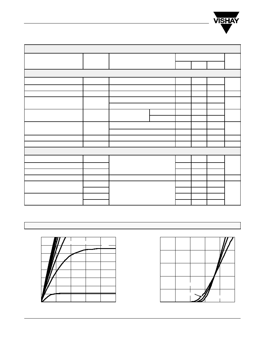
Output Characteristics
Transfer Characteristics
V
DS
- Drain-to-Source Voltage (V)
-
Drain Current (A)
I
D
V
GS
- Gate-to-Source Voltage (V)
-
Drain Current (A)
I
D
4 V
2 V

TN0201K/TN0201KL
Vishay Siliconix
New Product
Document Number: 72671
S-40245--Rev. A, 16-Feb-04
www.vishay.com
3
TYPICAL CHARACTERISTICS (25_C UNLESS NOTED)
0.0
0.2
0.4
0.6
0.8
1.0
1.2
1.4
-
On-Resistance (
r
DS(on)
W
)
0
10
20
30
40
50
0
4
8
12
16
20
0.6
0.8
1.0
1.2
1.4
1.6
-50
-25
0
25
50
75
100
125
150
0
2
4
6
8
10
0.0
0.2
0.4
0.6
0.8
1.0
0.0
0.3
0.6
0.9
1.2
1.5
0.0
0.1
0.2
0.3
0.4
0.5
0.6
0.7
0.8
V
DS
- Drain-to-Source Voltage (V)
C
rss
C
oss
C
iss
V
DS
= 16 V
I
D
= 0.3 A
I
D
- Drain Current (A)
V
GS
= 4.5 V
I
D
= 0.1 A
V
GS
= 10 V
Gate Charge
On-Resistance vs. Drain Current
-
Gate-to-Source V
oltage (V)
Q
g
- Total Gate Charge (nC)
C
-
Capacitance (pF)
V
GS
Capacitance
On-Resistance vs. Junction Temperature
T
J
- Junction Temperature (_C)
(Normalized)
-
On-Resistance (
r
DS(on)
W
)
0.0
0.4
0.8
1.2
1.6
2.0
2.4
0
4
8
12
16
20
T
J
= 150_C
T
J
= 25_C
I
D
= 0.3 A
3
0.1
0.001
Source-Drain Diode Forward Voltage
On-Resistance vs. Gate-to-Source Voltage
-
On-Resistance (
r
DS(on)
W
)
V
SD
- Source-to-Drain Voltage (V)
V
GS
- Gate-to-Source Voltage (V)
-
Source Current (A)
I
S
V
GS
= 4.5 V
V
GS
= 10 V
I
D
= 0.3 A
1
0.01

TN0201K/TN0201KL
Vishay Siliconix
New Product
www.vishay.com
4
Document Number: 72671
S-40245--Rev. A, 16-Feb-04
TYPICAL CHARACTERISTICS (25_C UNLESS NOTED)
10
-3
10
-2
1
10
600
10
-1
10
-4
100
-0.6
-0.4
-0.2
-0.0
0.2
0.4
-50
-25
0
25
50
75
100
125
150
I
D
= 250 mA
2
1
0.1
0.01
0.2
0.1
0.05
0.02
Single Pulse
Duty Cycle = 0.5
Threshold Voltage
V
ariance (V)
V
GS(th)
T
J
- Temperature (_C)
Normalized Thermal Transient Impedance, Junction-to-Ambient (TO-236, TN0201K Only)
Square Wave Pulse Duration (sec)
Normalized Ef
fective
T
ransient
Thermal Impedance
Safe Operating Area (TO-236, TN0201K Only)
V
DS
- Drain-to-Source Voltage (V)
10
0.1
0.1
1
10
100
0.001
1
1 ms
-
Drain Current (A)
I
D
0.01
T
A
= 25_C
Single Pulse
10 ms
100 ms
dc
1 s
10 s
Safe Operating Area (TO-226AA, TN0201KL Only)
I
D(on)
Limited
r
DS(on)
Limited
BV
DSS
Limited
V
DS
- Drain-to-Source Voltage (V)
10
0.1
0.1
1
10
100
0.001
1
1 ms
-
Drain Current (A)
I
D
0.01
T
A
= 25_C
Single Pulse
10 ms
100 ms
dc
1 s
10 s
I
D(on)
Limited
I
DM
Limited
r
DS(on)
Limited
I
DM
Limited
BV
DSS
Limited

TN0201K/TN0201KL
Vishay Siliconix
New Product
Document Number: 72671
S-40245--Rev. A, 16-Feb-04
www.vishay.com
5
TYPICAL CHARACTERISTICS (25_C UNLESS NOTED)
10
-3
10
-2
1
10
600
10
-1
10
-4
100
2
1
0.1
0.01
0.2
0.1
0.05
0.02
Single Pulse
Duty Cycle = 0.5
Normalized Thermal Transient Impedance, Junction-to-Ambient (TO-226AA, TN0201KL Only)
Square Wave Pulse Duration (sec)
Normalized Ef
fe
ctive T
ransient
Thermal Impedance